


Combination of common-source grounded emitter amplifier
#common-source
#grounded emitter
#radio amplifier
#input impedance
#transistor
#signal amplification
#audio
#RF
#electronic circuit
#impedance matching

Description: A combination of a common-source grounded emitter amplifier and a common emitter amplifier. The input impedance of the common emitter amplifier is in the range of 1.03 fl. Directly connecting the FET drive can be challenging; however, utilizing an emitter follower as illustrated allows for easier driving. The load resistance is connected to the common emitter amplifier, facilitating this integration. The output stage circuit incorporates the emitter follower to achieve current gain, exemplifying a typical low output impedance.
The described circuit integrates a common-source amplifier and a common emitter amplifier configuration to enhance the overall performance of the signal amplification process. The common-source amplifier, typically used in FET-based designs, provides high voltage gain, while the common emitter amplifier offers a balance of voltage and current gain with moderate input impedance.
In this configuration, the common emitter amplifier's input impedance is approximately 1.03 ohms, which presents a challenge for direct connections from the FET drive. To mitigate this issue, an emitter follower stage is introduced. The emitter follower, known for its high input impedance and low output impedance, serves as a buffer that allows for seamless interfacing between the FET and the common emitter amplifier. This configuration enhances the drive capability of the circuit, ensuring that the signal can be effectively transmitted without significant loss.
The load resistance (R_Tuen) is strategically connected to the common emitter amplifier to optimize the performance of the amplifier system. The inclusion of the emitter follower stage not only facilitates current gain but also stabilizes the output impedance, making it suitable for driving subsequent stages or loads that require a low impedance drive. This design exemplifies a robust approach to amplifier design, ensuring that both voltage and current gains are achieved while maintaining signal integrity and minimizing distortion.
Overall, this combination of amplifiers is ideal for applications requiring reliable amplification with efficient power handling, making it a valuable configuration in electronic circuit design. Combination of common-source grounded emitter amplifier A combination of common-source grounded pole radio amplifier. Common emitter amplifier input impedance in the range of l 03fl, it is difficult straight from the FET drive connected, however, if level through emitter follower, which as shown in FIG load R Tuen, connected to the common emitter amplifier the former, it is easy to drive, and as shown in FIG. The output stage circuit in front of the stage to join the emitter follower to get current gain, is an example of a typical low output impedance.
The described circuit integrates a common-source amplifier and a common emitter amplifier configuration to enhance the overall performance of the signal amplification process. The common-source amplifier, typically used in FET-based designs, provides high voltage gain, while the common emitter amplifier offers a balance of voltage and current gain with moderate input impedance.
In this configuration, the common emitter amplifier's input impedance is approximately 1.03 ohms, which presents a challenge for direct connections from the FET drive. To mitigate this issue, an emitter follower stage is introduced. The emitter follower, known for its high input impedance and low output impedance, serves as a buffer that allows for seamless interfacing between the FET and the common emitter amplifier. This configuration enhances the drive capability of the circuit, ensuring that the signal can be effectively transmitted without significant loss.
The load resistance (R_Tuen) is strategically connected to the common emitter amplifier to optimize the performance of the amplifier system. The inclusion of the emitter follower stage not only facilitates current gain but also stabilizes the output impedance, making it suitable for driving subsequent stages or loads that require a low impedance drive. This design exemplifies a robust approach to amplifier design, ensuring that both voltage and current gains are achieved while maintaining signal integrity and minimizing distortion.
Overall, this combination of amplifiers is ideal for applications requiring reliable amplification with efficient power handling, making it a valuable configuration in electronic circuit design. Combination of common-source grounded emitter amplifier A combination of common-source grounded pole radio amplifier. Common emitter amplifier input impedance in the range of l 03fl, it is difficult straight from the FET drive connected, however, if level through emitter follower, which as shown in FIG load R Tuen, connected to the common emitter amplifier the former, it is easy to drive, and as shown in FIG. The output stage circuit in front of the stage to join the emitter follower to get current gain, is an example of a typical low output impedance.

simple sound to light converter schematic
A simple circuit for converting an audio signal (such as one that comes from the output terminals of a CD player). The circuit basically consists of a buffer/amplifier stage and three filter circuits: a high-pass filter, a mid-pass filter, and...
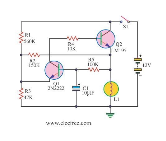
A lamp flasher circuit using transistors
If you require a small lamp that flashes for general use, there are numerous options available. Today, three lamp flasher circuits will be presented.
The three lamp flasher circuits can be designed using different components and configurations, each offering unique characteristics...

Three of the five band equalizer circuit transistor
Figure 4-33 illustrates a circuit configuration that includes a common amplifier along with analog inductive circuits. In this setup, the transistor in the analog inductive circuit is utilized, and an increase in the bias resistor enhances circuit stability. A potentiometer...
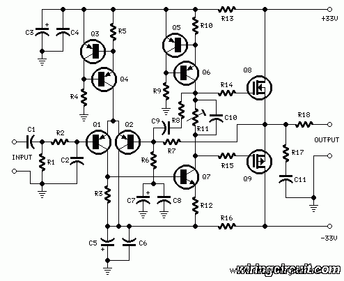
25W HiFi Audio Amplifier with MOSFET
This is a high-fidelity, high-quality audio amplifier circuit diagram. A pre-amplifier is not required. Component list: R1, R4 = 47K 1/4W resistors; R2 = 4.7K 1/4W resistor; R3 = 1.5K 1/4W resistor; R5 = 390Ω 1/4W resistor; R6 = 470Ω...

Example Transistor Circuit with LEDs
A transistor is an electronic component that allows a small current to control a significantly larger current. This characteristic is valuable in various renewable energy projects and other applications. A basic circuit diagram is provided, featuring a 12V LED spotlight...

RF field strength meter
A simple Field Strength Meter consists of a small antenna, a detector diode, a resistor, a capacitor, and a micro ammeter. This circuit is sensitive enough to detect HF fields when positioned close to the transmitting antenna. The circuit functioned...

Simple Two-Transistor Motorcycle Alarm
When one of the switches is closed, the base of Q1 is connected to ground through D1 and R2. This activates Q1, which in turn activates Q2. Q2 connects the positive side of the relay coil to the supply line,...

Power Control
The circuit presented utilizes a two-transistor "flasher" to generate triggering pulses, replacing the traditional unijunction transistor design. This configuration allows for a broad range of control with minimal hysteresis and sensitivity to line voltage. Two diodes rectify the line voltage,...

Reverse Bias Oscillators
Several NPN transistors can oscillate within the audio frequency range when reverse biased. The minimum supply voltage required is 7V for low-power transistors like the BC109, BC238, and 2N2222A; it increases to 12V for medium-power transistors such as the BD139,...