


DC-coupled multi-stage amplifier circuit a
#DC-coupled
#multi-stage
#amplifier
#NPN transistor
#transistor circuits
#signal amplification
#electronic amplifier
#audio circuits

Description: A multi-stage DC-coupled amplifier circuit utilizes NPN type transistors. Each stage is designed to achieve an appropriate operating point at the base, resulting in a stepwise increase in collector potential, which subsequently reduces the final output voltage range. To address this issue, a combination of NPN and PNP transistors can be employed to lower the DC potential of the post-stage. For example, an NPN transistor (VT1) and a PNP transistor (VT2) can be used to decrease the potential of the following stage (VT3). Alternatively, an emitter follower stage can be utilized to amplify voltage while reducing the DC potential of the circuit.
The multi-stage DC-coupled amplifier circuit is designed to provide significant amplification while maintaining stability and linearity across its operational range. The use of NPN transistors in the initial stages allows for efficient amplification of the input signal. Each stage is configured to ensure that the biasing conditions are optimized, allowing the amplifier to operate effectively without distortion.
As the signal progresses through each stage, the collector potential incrementally rises. However, this increase in potential can lead to a reduction in the overall output voltage range, which may limit the circuit's performance in certain applications. To mitigate this effect, the implementation of PNP transistors in conjunction with NPN transistors is a common practice. The PNP transistor (VT2) can effectively lower the DC potential of the subsequent stage (VT3), allowing for a more manageable output voltage range.
In addition to using complementary transistor configurations, the circuit can also incorporate an emitter follower stage. This configuration serves as a buffer that provides voltage gain while simultaneously reducing the DC potential seen by the following stages. The emitter follower is characterized by its high input impedance and low output impedance, making it an ideal choice for interfacing between stages of an amplifier.
In summary, the multi-stage DC-coupled amplifier circuit leverages the properties of both NPN and PNP transistors to achieve a robust amplification solution, while the inclusion of emitter follower stages enhances the circuit's overall performance by managing DC levels effectively.DC-coupled multi-stage amplifier circuit a (3) multi-stage DC-coupled amplifier in DC-coupled by a multi-stage amplifier circuit amplifying circuit, if used NPN type transistor of each stage, in order to fit all levels have appropriate operating point of stage base, Step by step the collector potential increases, so reducing the final output voltage range. In order to solve this problem, in practice, it can be used in conjunction with NPN and PNP transistor to reduce the post-stage DC potential, as shown in FIG.
Figure (8) shows an NPN cvri) and PNP transistor (VT2) wish, is used to reduce the subsequent stage (VT3) potential. Alternatively, you can use emitter follower, stage amplified voltage diode to reduce a DC potential of the circuit.
Figure l-43 (b) shows the use of emitter cvn) is used to reduce the subsequent stage (, rr3) potential.
The multi-stage DC-coupled amplifier circuit is designed to provide significant amplification while maintaining stability and linearity across its operational range. The use of NPN transistors in the initial stages allows for efficient amplification of the input signal. Each stage is configured to ensure that the biasing conditions are optimized, allowing the amplifier to operate effectively without distortion.
As the signal progresses through each stage, the collector potential incrementally rises. However, this increase in potential can lead to a reduction in the overall output voltage range, which may limit the circuit's performance in certain applications. To mitigate this effect, the implementation of PNP transistors in conjunction with NPN transistors is a common practice. The PNP transistor (VT2) can effectively lower the DC potential of the subsequent stage (VT3), allowing for a more manageable output voltage range.
In addition to using complementary transistor configurations, the circuit can also incorporate an emitter follower stage. This configuration serves as a buffer that provides voltage gain while simultaneously reducing the DC potential seen by the following stages. The emitter follower is characterized by its high input impedance and low output impedance, making it an ideal choice for interfacing between stages of an amplifier.
In summary, the multi-stage DC-coupled amplifier circuit leverages the properties of both NPN and PNP transistors to achieve a robust amplification solution, while the inclusion of emitter follower stages enhances the circuit's overall performance by managing DC levels effectively.DC-coupled multi-stage amplifier circuit a (3) multi-stage DC-coupled amplifier in DC-coupled by a multi-stage amplifier circuit amplifying circuit, if used NPN type transistor of each stage, in order to fit all levels have appropriate operating point of stage base, Step by step the collector potential increases, so reducing the final output voltage range. In order to solve this problem, in practice, it can be used in conjunction with NPN and PNP transistor to reduce the post-stage DC potential, as shown in FIG.
Figure (8) shows an NPN cvri) and PNP transistor (VT2) wish, is used to reduce the subsequent stage (VT3) potential. Alternatively, you can use emitter follower, stage amplified voltage diode to reduce a DC potential of the circuit.
Figure l-43 (b) shows the use of emitter cvn) is used to reduce the subsequent stage (, rr3) potential.

Amplifier Timer Circuit Schematic
This circuit turns off an amplifier or any other device when a low-level audio signal fed to its input is absent for at least 15 minutes. Pressing P1 switches the device on, supplying power to any appliance connected to SK1....

Bird Feeder Monitor Circuit
The first amplifier circuit is a bird phone. In this circuit, the electret microphone (MIC1) is mounted in the neck of a large plastic funnel. The amplifier, built around an MC34119, is then placed outside of the funnel with the...

A simple and effective short-wave antenna amplifier circuit
This amplifier is designed for outdoor installation and is connected to an indoor power line box. It utilizes either 50-ohm or 75-ohm coaxial cables for the connection between indoor and outdoor units. The amplifier circuit board is depicted in Figures...

5W-150mhz-amplifier
This circuit employs the MRF123 TMOS power FET. The MRF134 is a high-gain FET that may exhibit instability at both VHF and UHF frequencies. A 68-ohm input loading resistor has been used to improve stability. This amplifier achieves a gain...
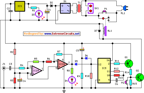
amplifier timer circuit schematic
This circuit deactivates an amplifier or any connected device when a low-level audio signal at its input is absent for at least 15 minutes. By pressing P1, the device is powered on, supplying power to any appliance connected to SK1....

DC-Coupled Audio Amplifier Circuit
This design circuit for audio amplifiers with DC coupling to the load is not commonly used today, despite its clear advantages. One advantage is the elimination of the need for a second (symmetric) power supply, and another is the improved...
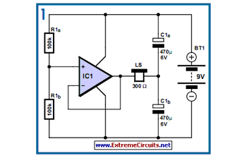
DC-Coupled Audio Amplifier
Designs for audio amplifiers with DC coupling to the load are not commonly seen today, despite their clear benefits. One advantage...
Audio amplifiers utilizing DC coupling to the load present several notable advantages in specific applications. DC coupling allows for a...

Emitter negative feedback differential amplifier gain control circuit
A controllable gain amplifier functions as an automatic gain control circuit within the execution unit. The primary methods for controlling the amplifier's gain involve two approaches: one is by adjusting certain parameters of the amplifier itself, such as emitter current,...

Amplifier Clipping Indicator
At some stage, we will all find ourselves pushing hi-fi equipment just a little too hard, and if lucky, will just find that the sound has become "dirty". If this happens too often or is too severe, tweeters are the...