


Low-distortion 1.6-30mhz ssb driver
#low-distortion
#SSB
#RF amplifier
#MRF476
#MRF475
#power gain
#IMD
#negative feedback
#bias adjustment

Description: The amplifier achieves a total power gain of approximately 25 dB, utilizing a construction technique that incorporates low-cost components throughout. The MRF476 is rated as a 3-watt device, while the MRF475 delivers an output power of 12 watts. Both devices demonstrate significant tolerance to overdrive and load mismatches, even under continuous wave (CW) conditions. Typical intermodulation distortion (IMD) figures are better than -35 dB, with power gains of 18 dB and 12 dB, respectively, at 30 MHz. The bias currents for each stage can be individually adjusted using resistors R5 and R6. Capacitors C4 and C10 serve as audio-frequency bypasses, effectively reducing the source impedance at modulation frequencies. Gain leveling across the frequency band is accomplished through simple RC networks connected in series with the bases, alongside negative feedback.
The amplitude of the out-of-phase voltages at the bases is inversely related to frequency due to the series inductance in the feedback loop and the increasing input impedance of the transistor at lower frequencies. In contrast, the negative feedback reduces the effective input impedance presented to the source (distinct from the device's own input impedance), and with the correct voltage slope, it can be equalized. This method enables the maintenance of an input voltage standing wave ratio (VSWR) of 1.5:1 or less, up to 30 MHz.
The described amplifier circuit is designed for efficiency and performance, particularly in RF applications. The use of MRF476 and MRF475 transistors allows for robust operation, ensuring minimal distortion and high linearity. The adjustable bias currents facilitate fine-tuning of the amplifier's performance, accommodating variations in component tolerances and operating conditions. The capacitors employed for audio-frequency bypassing are critical in maintaining signal integrity and minimizing unwanted feedback that could adversely affect performance.
The RC networks used for gain leveling are strategically placed to provide a smooth response across the operating frequency range. This design choice is essential for applications requiring consistent gain characteristics, particularly in communication systems where signal fidelity is paramount. The negative feedback mechanism not only improves stability but also enhances the amplifier's ability to handle varying load conditions without significant degradation in performance.
Overall, this amplifier design exemplifies a careful balance between cost-efficiency and high-performance metrics, making it suitable for a wide range of applications in the RF spectrum. Proper implementation of this circuit can yield reliable operation with minimal maintenance, making it an attractive option for both commercial and amateur radio applications.The amplifier provides a total power gain of about 25 dB, and the construction technique allows the use of inexpensive components throughout. The MRF476 is specified as a 3 watt device and the MRF475 has an output power of 12 watts. Both are extremely tolerant to overdrive and load mismatches, even under CW conditions. Typical IMD numbers are better than -35 dB, and the power gains are 18 dB and 12 dB, respectively, at 30 MHz.
The bias currents of each stage are individually adjustable with R5 and R6. Capacitors C4 and CIO function as audio-frequency bypasses to further reduce the source impedance at the frequencies of modulation. Gain leveling across the band is achieved with simple RC networks in series with the bases, in conjunction with negative feedback.
The amplitude of the out-of-phase voltages at the bases is inversely proportional to the frequency as a result of the series inductance in the feedback loop and the increasing input impedance of the transistor at low frequencies. Conversely, the negative feedback lowers the effective input impedance presented to the source (not the input impedance of the device itself) and with proper voltage slope would equalize it.
With this technique, it is possible to maintain an input VSWR of 1.5:1 or less than 1.6 to 30 MHz.
The amplitude of the out-of-phase voltages at the bases is inversely related to frequency due to the series inductance in the feedback loop and the increasing input impedance of the transistor at lower frequencies. In contrast, the negative feedback reduces the effective input impedance presented to the source (distinct from the device's own input impedance), and with the correct voltage slope, it can be equalized. This method enables the maintenance of an input voltage standing wave ratio (VSWR) of 1.5:1 or less, up to 30 MHz.
The described amplifier circuit is designed for efficiency and performance, particularly in RF applications. The use of MRF476 and MRF475 transistors allows for robust operation, ensuring minimal distortion and high linearity. The adjustable bias currents facilitate fine-tuning of the amplifier's performance, accommodating variations in component tolerances and operating conditions. The capacitors employed for audio-frequency bypassing are critical in maintaining signal integrity and minimizing unwanted feedback that could adversely affect performance.
The RC networks used for gain leveling are strategically placed to provide a smooth response across the operating frequency range. This design choice is essential for applications requiring consistent gain characteristics, particularly in communication systems where signal fidelity is paramount. The negative feedback mechanism not only improves stability but also enhances the amplifier's ability to handle varying load conditions without significant degradation in performance.
Overall, this amplifier design exemplifies a careful balance between cost-efficiency and high-performance metrics, making it suitable for a wide range of applications in the RF spectrum. Proper implementation of this circuit can yield reliable operation with minimal maintenance, making it an attractive option for both commercial and amateur radio applications.The amplifier provides a total power gain of about 25 dB, and the construction technique allows the use of inexpensive components throughout. The MRF476 is specified as a 3 watt device and the MRF475 has an output power of 12 watts. Both are extremely tolerant to overdrive and load mismatches, even under CW conditions. Typical IMD numbers are better than -35 dB, and the power gains are 18 dB and 12 dB, respectively, at 30 MHz.
The bias currents of each stage are individually adjustable with R5 and R6. Capacitors C4 and CIO function as audio-frequency bypasses to further reduce the source impedance at the frequencies of modulation. Gain leveling across the band is achieved with simple RC networks in series with the bases, in conjunction with negative feedback.
The amplitude of the out-of-phase voltages at the bases is inversely proportional to the frequency as a result of the series inductance in the feedback loop and the increasing input impedance of the transistor at low frequencies. Conversely, the negative feedback lowers the effective input impedance presented to the source (not the input impedance of the device itself) and with proper voltage slope would equalize it.
With this technique, it is possible to maintain an input VSWR of 1.5:1 or less than 1.6 to 30 MHz.

Broadcast band RF amplifier
The circuit exhibits a frequency response that spans from 100 Hz to 3 MHz, with a gain of approximately 30 dB. The field-effect transistor Q1 is arranged in a common-source self-biased configuration, while an optional resistor R1 allows for the...

1 500-W Rf Amplifier
The frequency range of this amplifier is 1.8 to 54 MHz. The required RF drive for full output is approximately 30 W. The grid compartment (Rl, R2, RFC4, RFC5) must be shielded from other circuitry, particularly the output circuitry. Capacitors...
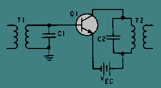
RF amplifier coupling
There are various methods to couple signals from one stage to another. Transformer coupling is the most prevalent technique employed for coupling RF amplifiers. Transformer coupling offers numerous advantages over RC coupling for RF amplifiers; for instance, it utilizes fewer...

TV signal amplifier 470Mhz-860Mhz
This amplifier is designed to amplify RF signals from an antenna by 10 dB and operates as a Class A amplifier using the BFQ34 transistor from Philips. The BFQ34 is packaged in an SOT122A case. The BFQ34T variant is available...

RF2103P schematic configuration of 915MHz RF amplifier
The circuit illustrated in FIG consists of the RF2103P 915MHz RF amplifier circuit. P1 serves as the outlet, where P1-1 connects to power Vcc, P1-2 connects to ground, and P1-3 is used for the power down control voltage VB. J1...

Broadcast Band Rf Amplifier Circuit
The circuit features a frequency response that spans from 100 Hz to 3 MHz, with a gain of approximately 30 dB. Field-effect transistor Q1 is arranged in a common-source self-biased configuration, and an optional resistor R1 is available to adjust...

broadcast band rf amplifier
The circuit features a frequency response from 100 Hz to 3 MHz, with a gain of approximately 30 dB. The field-effect transistor Q1 is configured in a common-source self-biased mode. An optional resistor R1 allows for the adjustment of the...

15w rf amplifier circuit
An RF power amplifier is a type of electronic amplifier used to convert a low-power radio-frequency signal into a larger signal of significant power, typically for driving the antenna of a transmitter. It is optimized for high efficiency, high output...

BLY94 50W RF Amplifier Circuit
This FM RF power amplifier circuit is constructed using a BLY94 transistor, which can deliver up to 50W at a frequency of 175MHz with a power gain of 7dB, resulting in approximately 5 times power amplification. However, in this schematic,...