


Variable gain amplifier circuit
#variable gain
#amplifier
#signal amplitude
#controllable
#output signal
#input signal
#gain control

Description: A variable gain amplifier is presented. This circuit adjusts the output signal amplitude based on the input signal. The core component is an operational amplifier configured with a negative feedback circuit. By varying the feedback amount, the gain of the amplifier can be modified. The design features a control terminal utilizing a double gate field effect transistor, specifically the PIX429D, which serves as the negative feedback control element. The control voltage can vary from -10 V to -2 V, resulting in an output range that changes from 220 mV to 2.2 V.
The variable gain amplifier operates by utilizing an operational amplifier (op-amp) at its core. The op-amp is configured in a negative feedback arrangement, which is essential for controlling the gain. The feedback loop is adjusted by manipulating the feedback resistor, which is influenced by the control voltage applied to the double gate field effect transistor (FET) PIX429D.
The operational amplifier amplifies the input signal based on the gain set by the feedback network. The gain can be expressed as the ratio of the output voltage to the input voltage. By altering the control voltage applied to the FET, the resistance in the feedback path changes, allowing for a dynamic adjustment of the gain. This allows the output voltage to vary within a specified range, in this case, from 220 mV to 2.2 V, depending on the control voltage level.
The operational amplifier's performance characteristics, such as bandwidth, slew rate, and noise figure, are critical in determining the overall effectiveness of the variable gain amplifier. The design should ensure that the op-amp operates within its linear range to avoid distortion of the amplified signal. Additionally, the choice of the PIX429D FET is crucial, as it must provide adequate control over the feedback mechanism without introducing significant noise or delay.
Overall, this variable gain amplifier design offers flexibility in signal processing applications, where adjustable gain is necessary to accommodate varying input signal levels while maintaining signal integrity.Variable gain amplifier Shown is a variable gain amplifier. For fixing the input signal, the output signal amplitude of the controllable amplifier circuit. The electrical main road is an operational amplifier, negative feedback circuit by changing the amount of feedback to change the gain of the amplifier, the figure having a base control terminal double gate field effect transistor PIX429D negative feedback control device, the control voltage -10 to - 2 V of the change between, making the output between 220 mV ~ 2.2 V change.
The variable gain amplifier operates by utilizing an operational amplifier (op-amp) at its core. The op-amp is configured in a negative feedback arrangement, which is essential for controlling the gain. The feedback loop is adjusted by manipulating the feedback resistor, which is influenced by the control voltage applied to the double gate field effect transistor (FET) PIX429D.
The operational amplifier amplifies the input signal based on the gain set by the feedback network. The gain can be expressed as the ratio of the output voltage to the input voltage. By altering the control voltage applied to the FET, the resistance in the feedback path changes, allowing for a dynamic adjustment of the gain. This allows the output voltage to vary within a specified range, in this case, from 220 mV to 2.2 V, depending on the control voltage level.
The operational amplifier's performance characteristics, such as bandwidth, slew rate, and noise figure, are critical in determining the overall effectiveness of the variable gain amplifier. The design should ensure that the op-amp operates within its linear range to avoid distortion of the amplified signal. Additionally, the choice of the PIX429D FET is crucial, as it must provide adequate control over the feedback mechanism without introducing significant noise or delay.
Overall, this variable gain amplifier design offers flexibility in signal processing applications, where adjustable gain is necessary to accommodate varying input signal levels while maintaining signal integrity.Variable gain amplifier Shown is a variable gain amplifier. For fixing the input signal, the output signal amplitude of the controllable amplifier circuit. The electrical main road is an operational amplifier, negative feedback circuit by changing the amount of feedback to change the gain of the amplifier, the figure having a base control terminal double gate field effect transistor PIX429D negative feedback control device, the control voltage -10 to - 2 V of the change between, making the output between 220 mV ~ 2.2 V change.

Amplifier Compressor MC3340P
The output is rectified, and TR2 controls the gain of the ICL. This audio compressor circuit uses an MC3340P as a variable gain amplifier.
The audio compressor circuit described utilizes an MC3340P integrated circuit, which functions as a variable gain amplifier...

Amplifier Output Delay with Relay Schematic Diagram
This is a minimal circuit designed for individual audio amplifier projects to control the presenter output relay. The purpose of this circuit is to manage the relay that activates the speaker output within the audio amplifier. The circuit introduces a...

A simple and effective short-wave antenna amplifier circuit
This amplifier is designed for outdoor installation and is connected to an indoor power line box. It utilizes either 50-ohm or 75-ohm coaxial cables for the connection between indoor and outdoor units. The amplifier circuit board is depicted in Figures...

Wide band high frequency amplifier circuit
This is a wideband high-frequency amplifier circuit designed for a frequency range between 75-150 MHz. It utilizes a PNP transistor amplifier to enhance signal strength before it reaches the receiver of devices such as phones, FM radios, or amateur radios....
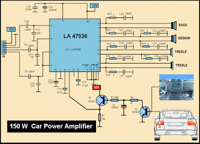
Schematic MP3 Car Audio Power AmplifierCircuits
This is a diagram of a car audio active loudspeaker utilizing the LF353 operational amplifier from National Semiconductor. For optimal performance, the NE5532 is recommended to split the audio signal into three frequency bands using an active filter. The SANYO...

Amplifier Bridging
The primary advantage of this method of bridging is that no additional components are needed, which means that it is cheap, and there is no signal degradation from additional opamps in the circuit path. The results are at least as...

Common intermediate frequency amplifier circuit having a circuit and on the radio
A common intermediate frequency amplifier circuit is presented, along with its components and parameters. The reference values for the components are as follows: 1) Transistors: VT1 to 3DG19, Vcc = 6V. 2) Resistance values: R1 = 50 kΩ, R2 =...

RECEIVER BUILDING BLOCKS
This amplifier has about 20dB of gain, bandwidth of 100MHz and noise figure of about 7dB. The output transformer is 8 turns bifilar wound on a ferrite core. Use a medium power UHF transistor 2N5109, 2N3866, 2N4427 or similar. The...
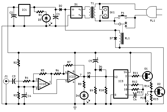
Amplifier Timer
This circuit deactivates an amplifier or other devices when a low-level audio signal at its input is absent for at least 15 minutes. By pressing P1, the device is activated, supplying power to any appliance connected to SK1. The input...