


Variable gain differential amplifier circuit diagram A709
#differential amplifier
#variable gain
#A709
#CMRR
#operational amplifier
#signal processing
#analog circuit
#gain control
#electronic design
#circuit diagram

Description: The configuration of the variable gain A709 differential amplifier circuit is illustrated. The primary advantage of this circuit is its ability to maintain a constant common-mode rejection ratio (CMRR) while allowing for continuous adjustments to the differential gain. The circuit utilizes four resistors, with resistors R2 and R1 required to have equal resistance values. The accompanying numerical figures demonstrate typical application scenarios. By adjusting potentiometer R3, continuous voltage amplification can be achieved. For instance, when the gain adjustment resistor R3 is set to 5, the corresponding ratio of R2 to R3 is 104, resulting in a voltage amplification (Av) of -104, calculated using the formula Av = 2R2/R1. The circuit offers a wide and easily adjustable gain range. However, it is important to note that excessive voltage gain can lead to significant nonlinear distortion as the output voltage approaches the power supply voltage. Additionally, an RC compensation network is introduced between pins 1 and 8, and a compensation capacitor (C2) is connected between pins 5 and 6 to enhance circuit stability and prevent parasitic oscillations. The fundamental relationship governing the circuit is expressed as Vo = (2R2/R1)(1 + R2/R3)(Vi1 - Vi2), with the output voltage Vo related to the input voltages Vi1 and Vi2 as Vo/(Vi1 + Vi2) = (2R2/R1)(1 + R2/R3). For resistor values of R1 = 10k, R2 = 50k, and R3 = 5k, the resulting voltage amplification Av is -110. The electrical parameters of the A709 integrated chip are specified as VD = 15V and TA = 25°C.
The A709 differential amplifier circuit is designed to provide adjustable gain while maintaining high linearity and stability. By utilizing precision resistors for R1 and R2, the circuit ensures that the differential gain can be finely tuned without compromising the integrity of the signal. The resistive divider formed by R2 and R3 allows for a smooth transition in gain settings, making it suitable for applications requiring variable amplification.
The inclusion of the RC compensation network is essential for stabilizing the amplifier, particularly in high-frequency applications where parasitic capacitance can lead to unwanted oscillations. The choice of capacitor value for C2 is critical; it should be selected based on the desired bandwidth and stability margins of the amplifier. The relationship between the gain and the resistor values can be adjusted to optimize performance for specific applications, such as instrumentation or audio processing.
In practical implementations, attention must be paid to the power supply voltage to avoid saturation of the output. The design should ensure that the amplifier operates within its linear range, and proper decoupling capacitors should be used to minimize power supply noise, which can affect the performance of the circuit.
Overall, the A709 differential amplifier circuit stands out for its flexibility and performance, making it a valuable component in a variety of electronic systems where signal conditioning is required. As shown for the configuration of the variable gain A709 differential amplifier circuit. The biggest advantage of the circuit is in keeping CMRR KCMR same premise, continuously adjustable differential gain can be achieved. Circuit four resistors R2 and two resistors R1 resistance must be equal, respectively, the numerical figure shows the typical application time. Adjust potentiometer R3, can realize continuous adjustment voltage magnification. If the adjusted gain adjustment resistor R3 5, the corresponding ratio R2/R3 104, where the voltage amplification Av -104 (2R2/R1), the adjustment range of the apparent gain of the circuit is very wide and easy adjustment.
It needs to be emphasized that: the voltage gain is not too large, because when the gain is large Vo near the power supply voltage, the output voltage will be a serious nonlinear distortion. In addition, the introduction of a RC between pin 1,8 compensation branch, between pins 5 and 6 also introduces a compensation capacitor C2, to improve the stability of the circuit, to prevent parasitic oscillation.
The basic relationship of the circuit is: Vo - (2R2/R1) (1 + R2/R3) (Vi1-Vi2) Av Vo/(Vi1 a Vi2) - (2R2/R1) (1 + R2/R3) When R1 10k, R2 50k, R3 5k when, Av -110. A709 integrated chip electrical parameters (VD 15V, TA 25 )
The A709 differential amplifier circuit is designed to provide adjustable gain while maintaining high linearity and stability. By utilizing precision resistors for R1 and R2, the circuit ensures that the differential gain can be finely tuned without compromising the integrity of the signal. The resistive divider formed by R2 and R3 allows for a smooth transition in gain settings, making it suitable for applications requiring variable amplification.
The inclusion of the RC compensation network is essential for stabilizing the amplifier, particularly in high-frequency applications where parasitic capacitance can lead to unwanted oscillations. The choice of capacitor value for C2 is critical; it should be selected based on the desired bandwidth and stability margins of the amplifier. The relationship between the gain and the resistor values can be adjusted to optimize performance for specific applications, such as instrumentation or audio processing.
In practical implementations, attention must be paid to the power supply voltage to avoid saturation of the output. The design should ensure that the amplifier operates within its linear range, and proper decoupling capacitors should be used to minimize power supply noise, which can affect the performance of the circuit.
Overall, the A709 differential amplifier circuit stands out for its flexibility and performance, making it a valuable component in a variety of electronic systems where signal conditioning is required. As shown for the configuration of the variable gain A709 differential amplifier circuit. The biggest advantage of the circuit is in keeping CMRR KCMR same premise, continuously adjustable differential gain can be achieved. Circuit four resistors R2 and two resistors R1 resistance must be equal, respectively, the numerical figure shows the typical application time. Adjust potentiometer R3, can realize continuous adjustment voltage magnification. If the adjusted gain adjustment resistor R3 5, the corresponding ratio R2/R3 104, where the voltage amplification Av -104 (2R2/R1), the adjustment range of the apparent gain of the circuit is very wide and easy adjustment.
It needs to be emphasized that: the voltage gain is not too large, because when the gain is large Vo near the power supply voltage, the output voltage will be a serious nonlinear distortion. In addition, the introduction of a RC between pin 1,8 compensation branch, between pins 5 and 6 also introduces a compensation capacitor C2, to improve the stability of the circuit, to prevent parasitic oscillation.
The basic relationship of the circuit is: Vo - (2R2/R1) (1 + R2/R3) (Vi1-Vi2) Av Vo/(Vi1 a Vi2) - (2R2/R1) (1 + R2/R3) When R1 10k, R2 50k, R3 5k when, Av -110. A709 integrated chip electrical parameters (VD 15V, TA 25 )

Differential amplifier circuit four connection methods and features comparison b
A comparison of four connection methods and features of a differential amplifier circuit is presented. The circuit demonstrates a magnification of a single tube with half the earnings, effectively countering common-mode negative feedback effects. The Common-Mode Rejection Ratio (CMRR) remains...
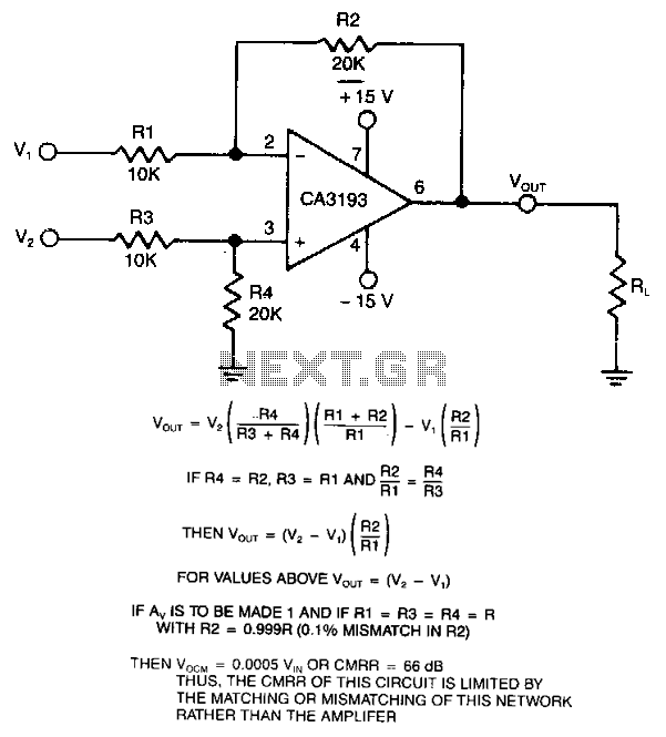
Differential-amplifier
This differential amplifier utilizes a CA3193 BiMOS operational amplifier. It serves as a classical differential input-to-signal-ended output converter, which, when paired with a low-resistance signal source, will sustain a high common-mode rejection ratio (CMRR), provided that R1 equals R3 plus...

Homemade whole integrated circuit amplifiers 01
The circuit depicted in Figure 5-60 and Figure 6 utilizes an operational amplifier (op-amp) configured as a channel pre-amplifier to address the signal loss introduced by the tone control circuit. Additionally, another group of op-amps forms a channel-driven stage amplifier...

Having a differential amplifier and overcurrent protection for power supply circuit 2
The circuit features a current protection mechanism utilizing transistors VTa, VT4, and a sense resistor Ro. When an overcurrent or short-circuit fault occurs, the power supply cannot resume normal operation because the conduction condition of VT3 remains unchanged, resulting in...

Common mode input voltage of the differential amplifier circuit diagram up l00V
Common mode input voltage up to a difference of 100V enlarged circuit diagram.
The circuit diagram described features a design capable of handling a common mode input voltage with a differential range of up to 100V. Such a configuration is essential...

lowvoltage ac voltmeter
The primary component of this circuit is an operational amplifier (such as the 741 or 351), configured as an amplifier with a feedback circuit that consists of a diode bridge full-wave rectifier. An ammeter is connected to the rectifier circuit,...

X10 operational amplifier
The amplifier is 3 dB down at 100 kHz and has a slew rate of 0.02 V/µs.
The amplifier's performance characteristics indicate that it experiences a 3 dB attenuation at a frequency of 100 kHz. This specification suggests that at this...

Analog circuit enforces slow servo response
The all-analog circuit presented controls the rate at which a miniature turbojet engine can be throttled. Increasing or decreasing the throttle too quickly on a miniature turbojet engine, or any jet engine, can lead to quick failure in flight, causing...

electronic design software for large electronics
The power supply unit (PSU) in question does not appear to be exceptionally large. Eagle software should be capable of managing these dimensions. The focus was more on finding an alternative that may already include the necessary components and be...