


Wide-range-digitally-controlled-variable-gain-amplifier
#LTC1043
#variable gain amplifier
#sampled data
#differential inputs
#gain stability
#switched-capacitor
#feedback resistor
#processor controlled
#1-kHz clock
#operational amplifier

Description: The circuit utilizes the LTC1043 in a variable gain amplifier configuration, which offers continuously adjustable gain, gain stability of 20 ppm/°C, and supports both single-ended and differential inputs. Two separate LTC1043 devices are employed in the design. The LTC1043B is continuously clocked by a 1-kHz source, which may also be supplied by a processor. Both LTC1043 devices operate as the sampled data equivalent of a resistor within the bandwidth defined by a 0.01 µF capacitor and the switched-capacitor equivalent feedback resistor. The time-averaged current delivered to the summing point by LTC1043A is determined by the input-derived voltage of the 0.01 µF capacitor and the commutation frequency at pin 16. Lower commutation frequencies yield smaller time-averaged current values, necessitating a larger input resistor, while higher frequencies require a correspondingly smaller input resistor.
The circuit design incorporates the LTC1043, a precision, low-drift, switched-capacitor technology component, which is pivotal in achieving the desired variable gain characteristics. The use of two LTC1043s allows for enhanced performance by separating the gain control and signal processing functions, facilitating greater flexibility in gain adjustment. The LTC1043B's continuous clocking at 1 kHz ensures that the signal processing remains responsive and stable, allowing for real-time adjustments to the gain based on input signal conditions.
The selection of a 0.01 µF capacitor is critical as it sets the bandwidth for the circuit, influencing the overall performance and response time. This capacitor, in conjunction with the switched-capacitor feedback resistor, forms a low-pass filter that determines the frequency response of the amplifier. The design must account for the trade-off between gain stability and bandwidth, as the gain stability of 20 ppm/°C ensures minimal drift with temperature variations, which is essential for precision applications.
The operational behavior of LTC1043A, in relation to the input voltage and commutation frequency, highlights the importance of selecting appropriate resistor values. The relationship between commutation frequency and input resistor size allows for tailored performance based on the specific application requirements. For instance, in scenarios where low frequencies are utilized, a larger input resistor is necessary to accommodate the lower time-averaged current, while higher frequencies can leverage smaller resistors for optimal performance.
Overall, this circuit exemplifies the application of advanced analog techniques to achieve precise control over gain in electronic systems, making it suitable for a variety of applications where signal integrity and stability are paramount.The circuit uses the LTC1043 in a variable gain amplifier which features continuously variable gain, gain stability of 20 ppm/°C, and single-ended or differential inputs. The circuit uses two separate LTC1043s. LTC1043B is continuously clocked by a 1-kHz source, which could also be processor supplied. Both LTC1043s function as the sampled data equivalent of a resistor within the bandwidth set by Al"s 0.01-I"F value and the switched-capacitor equivalent feedback resistor.
The time-averaged current delivered to the summing point by LTC1043A is a function of the 0.01-I"F capacitor"s input-derived voltage and the commutation frequency at pin 16. Low-commutation frequencies result in small time-averaged current values, and require a large input resistor.
Higher frequencies require an equivalent small input resistor.
The circuit design incorporates the LTC1043, a precision, low-drift, switched-capacitor technology component, which is pivotal in achieving the desired variable gain characteristics. The use of two LTC1043s allows for enhanced performance by separating the gain control and signal processing functions, facilitating greater flexibility in gain adjustment. The LTC1043B's continuous clocking at 1 kHz ensures that the signal processing remains responsive and stable, allowing for real-time adjustments to the gain based on input signal conditions.
The selection of a 0.01 µF capacitor is critical as it sets the bandwidth for the circuit, influencing the overall performance and response time. This capacitor, in conjunction with the switched-capacitor feedback resistor, forms a low-pass filter that determines the frequency response of the amplifier. The design must account for the trade-off between gain stability and bandwidth, as the gain stability of 20 ppm/°C ensures minimal drift with temperature variations, which is essential for precision applications.
The operational behavior of LTC1043A, in relation to the input voltage and commutation frequency, highlights the importance of selecting appropriate resistor values. The relationship between commutation frequency and input resistor size allows for tailored performance based on the specific application requirements. For instance, in scenarios where low frequencies are utilized, a larger input resistor is necessary to accommodate the lower time-averaged current, while higher frequencies can leverage smaller resistors for optimal performance.
Overall, this circuit exemplifies the application of advanced analog techniques to achieve precise control over gain in electronic systems, making it suitable for a variety of applications where signal integrity and stability are paramount.The circuit uses the LTC1043 in a variable gain amplifier which features continuously variable gain, gain stability of 20 ppm/°C, and single-ended or differential inputs. The circuit uses two separate LTC1043s. LTC1043B is continuously clocked by a 1-kHz source, which could also be processor supplied. Both LTC1043s function as the sampled data equivalent of a resistor within the bandwidth set by Al"s 0.01-I"F value and the switched-capacitor equivalent feedback resistor.
The time-averaged current delivered to the summing point by LTC1043A is a function of the 0.01-I"F capacitor"s input-derived voltage and the commutation frequency at pin 16. Low-commutation frequencies result in small time-averaged current values, and require a large input resistor.
Higher frequencies require an equivalent small input resistor.

TA-1500 fever amplifier circuit
Only the R channel is shown, with the original reference PCB label. Figure (a) illustrates the front tone circuit, which consists of a common negative feedback operational amplifier in an RC circuit configuration. The microphone signal is amplified by VTz,...

Precision current sink sourcel
An operational amplifier circuit can provide a constant voltage source with a high amplification factor and substantial load current. Even with significant variations in circuit parameters, the output voltage maintains high precision. The output current limit is managed by transistors...

Delay circuit of a multi-level output
A multi-stage delay circuit is presented in this schematic. The operational amplifiers are configured as comparators. Operational amplifier A1 operates when the voltage at the inverting input exceeds + VE. As the voltage at the inverting input of operational amplifiers...

A delay circuit using an operational amplifier
A delay circuit utilizing an operational amplifier functions as a comparator, providing high timing accuracy. The timer's delay range is from 1 to 30 seconds. The delay time is determined by resistors Ri, RP, and capacitor C. By adjusting RP,...

Class A Modular Preamplifier with Single Integrated Circuit
The circuit is based on a single operational amplifier integrated circuit designed to produce a modular preamplifier that operates in Class A configuration.
The modular preamplifier circuit utilizes a single operational amplifier (op-amp) integrated circuit, which serves as the primary amplification...

X100 operational amplifier
The amplifier has a gain-bandwidth product of 20 MHz, with a slew rate of 0.3 V/µs.
The amplifier's gain-bandwidth product (GBP) of 20 MHz indicates that the product of the amplifier's gain and the bandwidth at which that gain is applicable...

Homemade whole integrated circuit amplifiers 01
The circuit depicted in Figure 5-60 and Figure 6 utilizes an operational amplifier (op-amp) configured as a channel pre-amplifier to address the signal loss introduced by the tone control circuit. Additionally, another group of op-amps forms a channel-driven stage amplifier...
operational amplifier op amp oscillator
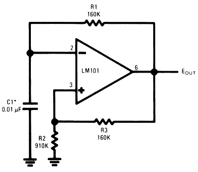
The timing capacitor (C1) generates multiple time constants, facilitating substantial voltage fluctuations at the input, attributable to the LM101's extensive input voltage range. It is advisable to decrease the value of resistor R2 and to increase the capacitance of C1...

Cosine wave Oscillator
This circuit is designed to output both a sine wave and a cosine wave. The design utilizes an operational amplifier, with the output frequency determined by component values set to 1Hz. The first operational amplifier generates a 1Hz sine wave,...