


CV/CC charger circuit diagram designed using LinKSwitch
#CV/CC charger
#LinKSwitch
#Power Integrations
#5V output
#650mA
#AC input
#rectifier
#power supply
#voltage regulator

Description: A simple 3.25W constant voltage/constant current (CV/CC) charger can be designed using the LinKSwitch family IC manufactured by Power Integrations. This electronic circuit project is intended to provide a 5-volt output with a maximum current of 650mA. The 3.25W CV/CC charger requires an AC input voltage ranging from 85 to 265 VAC. The AC input power is rectified by diodes D1 through D4. Bulk storage capacitors C1 and C2 filter the rectified AC. Inductor L1 forms a pi filter with C1 and C2 to attenuate conducted differential-mode EMI noise. The LinkSwitch-II device (U1) integrates the power switching device, an oscillator, a constant current/constant voltage control engine, startup circuitry, and protection functions into a single IC. The integrated 700V MOSFET provides sufficient voltage margin for universal input AC applications.
The described circuit is a compact and efficient solution for low-power charging applications. The LinKSwitch family IC serves as the core component, effectively managing the power conversion process while ensuring that the output remains stable under varying load conditions. The design utilizes a full-wave rectifier configuration with diodes D1 through D4, which converts the incoming AC voltage to a pulsating DC voltage. This rectified voltage is then smoothed out by the bulk capacitors C1 and C2, which serve to minimize voltage ripples and provide a stable DC output.
The inclusion of inductor L1 in conjunction with capacitors C1 and C2 forms a pi filter that is critical for reducing electromagnetic interference (EMI). This feature is particularly important in applications where sensitive electronic devices are present, as it helps to maintain compliance with EMI regulations and ensures reliable operation without interference.
The LinkSwitch-II IC, designated as U1 in the schematic, is a highly integrated solution that simplifies the design process. It combines several essential functions, including power switching, oscillation, and control, into a single package. This integration not only reduces the overall component count but also enhances the reliability of the circuit. The built-in 700V MOSFET provides adequate voltage headroom, allowing the charger to operate effectively across a wide range of input voltages, making it suitable for global applications.
Overall, this 3.25W CV/CC charger design exemplifies an efficient and reliable approach to power management, leveraging advanced semiconductor technology to deliver a stable output while minimizing size and complexity.A very simple 3. 25W CV/CC charger can be designed using LinKSwitch | family IC manufactured by Power Integrations. This electronic circuit project is designed to provide a 5 volts output at a maximum current of 650mA. This 3. 25W CV/CC charger, needs to be powered using a AC voltage between 85 and 265 VAC. The AC input power is rectified by dio des D1 through D4. Bulk storage capacitors C1 and C2 filter the rectified AC. Inductor L1 forms a pi ( ) filter with C1 and C2 to attenuate conducted differential-mode EMI noise. The LinkSwitch-II device (U1) incorporates the power switching device, an oscillator, a CC/CV control engine, startup circuitry, and protection functions into one IC. The integrated 700 V MOSFET allows sufficient voltage margin for universal input AC applications.
The described circuit is a compact and efficient solution for low-power charging applications. The LinKSwitch family IC serves as the core component, effectively managing the power conversion process while ensuring that the output remains stable under varying load conditions. The design utilizes a full-wave rectifier configuration with diodes D1 through D4, which converts the incoming AC voltage to a pulsating DC voltage. This rectified voltage is then smoothed out by the bulk capacitors C1 and C2, which serve to minimize voltage ripples and provide a stable DC output.
The inclusion of inductor L1 in conjunction with capacitors C1 and C2 forms a pi filter that is critical for reducing electromagnetic interference (EMI). This feature is particularly important in applications where sensitive electronic devices are present, as it helps to maintain compliance with EMI regulations and ensures reliable operation without interference.
The LinkSwitch-II IC, designated as U1 in the schematic, is a highly integrated solution that simplifies the design process. It combines several essential functions, including power switching, oscillation, and control, into a single package. This integration not only reduces the overall component count but also enhances the reliability of the circuit. The built-in 700V MOSFET provides adequate voltage headroom, allowing the charger to operate effectively across a wide range of input voltages, making it suitable for global applications.
Overall, this 3.25W CV/CC charger design exemplifies an efficient and reliable approach to power management, leveraging advanced semiconductor technology to deliver a stable output while minimizing size and complexity.A very simple 3. 25W CV/CC charger can be designed using LinKSwitch | family IC manufactured by Power Integrations. This electronic circuit project is designed to provide a 5 volts output at a maximum current of 650mA. This 3. 25W CV/CC charger, needs to be powered using a AC voltage between 85 and 265 VAC. The AC input power is rectified by dio des D1 through D4. Bulk storage capacitors C1 and C2 filter the rectified AC. Inductor L1 forms a pi ( ) filter with C1 and C2 to attenuate conducted differential-mode EMI noise. The LinkSwitch-II device (U1) incorporates the power switching device, an oscillator, a CC/CV control engine, startup circuitry, and protection functions into one IC. The integrated 700 V MOSFET allows sufficient voltage margin for universal input AC applications.

Low-forward-drop-rectifier-circuit
A TMOS power FET, Q1, and an LM393 comparator provide a high-efficiency rectifier circuit. When voltage V1 exceeds V2, the output of U1 becomes high, and Q1 conducts. Conversely, when V2 exceeds V1, the comparator output becomes low, and Q1...

LM7805 + 5V power supply configuration
The circuit illustrated in the figure provides an output voltage of +5V and an output current of 1.5A. It comprises a power transformer, a bridge rectifier circuit consisting of diodes D1 to D4, and filter capacitor C1. Additionally, capacitors C2...

stabilizer circuit
This circuit functions as a high-quality power supply with a continuously variable stabilized output that can be adjusted to any value between 0 and 30 VDC. It includes an electronic output current limiter that effectively regulates the output current from...
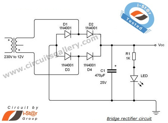
diode bridge rectifier circuits
A rectifier is an electronic circuit that converts AC voltage to DC voltage. It can be implemented using a combination of capacitors and diodes. The unique property of diodes, which allows current to flow in a single direction, is utilized...
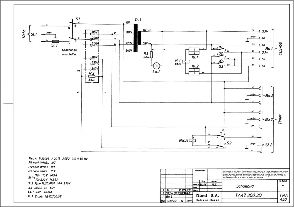
Durst power supplies EST 301 and EST 450
The regulator board of the ES301 has been inspected, revealing that the PCB contacts of the current sensing resistors R42 and R43 are severely burned. There is a nearby group of resistors that also need to be replaced, but their...

Three-terminal voltage regulator integrated fixed a typical wiring circuit
A fixed three-terminal integrated voltage regulator can be directly employed in various electronic devices as a voltage regulator. It features internal protections such as overcurrent protection, thermal protection, and safe operating area protection, making the circuit easy to use, safe,...

ISL6528 Dual Regulator-Standard Buck PWM and Linear Power Controller
The ISL6528 offers power control and protection for two output voltages in high-performance graphics cards and other embedded processor applications. This dual-output controller drives an N-Channel MOSFET in a standard buck topology and an NPN pass transistor in a linear...

Three-phase controlled rectifier circuit
Trigger circuit routing forms include various types such as simple trigger circuits, single-junction transistor trigger circuits, synchronous sine wave trigger circuits, sawtooth transition phase shift (synchronous) trigger circuits, and integrated trigger circuits. This section presents individual cases for introduction due...

12 Volt 30 Amp Power Supply
This power supply utilizes a single 7812 integrated circuit (IC) voltage regulator in conjunction with multiple external pass transistors to provide output load currents of up to 30 amps.
The circuit design incorporates a 7812 voltage regulator, which is known for...