


CW117 CW217 CW317 charger has a current-limiting protection configuration
#current-limiting
#transistor
#resistor
#protection circuit
#charger circuit
#CW117
#CW217
#CW317
#voltage regulation
#electronics

Description: The circuit depicted in the figure is a limiting protection charger. The VT transistors and resistor R3 create a limiting network. As illustrated, resistor R3 is connected in series with the battery being charged, acting as the emitter resistor for transistor VT. The charging current flows through resistor R3. If the charging current becomes excessive, the voltage drop across R3 will exceed 0.6V, causing transistor VT to turn on. Since VT is in parallel with resistor R2, its conduction decreases the equivalent parallel resistance, leading to a reduction in output voltage (Uo) and output current. This mechanism effectively limits the charging current. When R3 is set to a specific value, the maximum charging current can be calculated as Iom = 0.6/1 = 0.6A. Selecting a smaller R3 will increase the charging current but must not exceed the maximum output current rating of the integrated voltage regulator.
The limiting protection charger circuit utilizes a combination of transistors and resistors to regulate the charging current supplied to a battery. The core component of this circuit is the VT transistor, which functions as a switch that activates when the charging current surpasses a predetermined threshold. Resistor R3 plays a critical role in this setup, as it is placed in series with the battery and is responsible for sensing the charging current.
When the charging current flows through R3, it generates a voltage drop across the resistor. This voltage drop is directly proportional to the charging current, following Ohm's law (V = I × R). If this voltage drop exceeds the threshold of 0.6V, the transistor VT becomes forward-biased and turns on. The conduction of VT effectively alters the circuit's characteristics by providing a lower resistance path in parallel with resistor R2. As a result, the overall equivalent resistance of the circuit decreases, which in turn leads to a reduction in the output voltage (Uo) and consequently limits the output current delivered to the battery.
The design of this circuit allows for flexibility in setting the maximum charging current by adjusting the value of resistor R3. For instance, if R3 is chosen to be 1 ohm, the maximum charging current can be calculated as Iom = 0.6V / 1Ω = 0.6A. However, if a smaller resistor value is selected, the charging current will increase, but it is crucial to ensure that this does not exceed the maximum output current rating specified for the integrated voltage regulator used in the circuit. This careful consideration of component values is essential for maintaining the integrity and safety of the battery charging process. Overall, the limiting protection charger circuit is an effective solution for preventing overcurrent conditions during battery charging, thereby enhancing the longevity and reliability of the battery. As shown in Figure is a limiting protection charger. VT transistors and resistors R3 form limiting network. Seen from the figure, the resistor R3 is the base of transistor VT e mitter Q resistor connected in series with the battery being charged. Charging current flows through the resistor R3. When the charge current is too large, the voltage drop on R3 exceeds 0.6V, the transistor VT will be turned on. Because VT parallel with resistor R2, VT conduction, so that the equivalent parallel resistance decreases, the output voltage Uo decreases, the output current is reduced, so as to achieve the purpose of limiting the charging current.
When taken R3 l ), the maximum charging current is Iom 0.6/1 0.6A, select a smaller R3 will be higher charging current, but can not exceed the maximum integrated voltage regulator output current value.
The limiting protection charger circuit utilizes a combination of transistors and resistors to regulate the charging current supplied to a battery. The core component of this circuit is the VT transistor, which functions as a switch that activates when the charging current surpasses a predetermined threshold. Resistor R3 plays a critical role in this setup, as it is placed in series with the battery and is responsible for sensing the charging current.
When the charging current flows through R3, it generates a voltage drop across the resistor. This voltage drop is directly proportional to the charging current, following Ohm's law (V = I × R). If this voltage drop exceeds the threshold of 0.6V, the transistor VT becomes forward-biased and turns on. The conduction of VT effectively alters the circuit's characteristics by providing a lower resistance path in parallel with resistor R2. As a result, the overall equivalent resistance of the circuit decreases, which in turn leads to a reduction in the output voltage (Uo) and consequently limits the output current delivered to the battery.
The design of this circuit allows for flexibility in setting the maximum charging current by adjusting the value of resistor R3. For instance, if R3 is chosen to be 1 ohm, the maximum charging current can be calculated as Iom = 0.6V / 1Ω = 0.6A. However, if a smaller resistor value is selected, the charging current will increase, but it is crucial to ensure that this does not exceed the maximum output current rating specified for the integrated voltage regulator used in the circuit. This careful consideration of component values is essential for maintaining the integrity and safety of the battery charging process. Overall, the limiting protection charger circuit is an effective solution for preventing overcurrent conditions during battery charging, thereby enhancing the longevity and reliability of the battery. As shown in Figure is a limiting protection charger. VT transistors and resistors R3 form limiting network. Seen from the figure, the resistor R3 is the base of transistor VT e mitter Q resistor connected in series with the battery being charged. Charging current flows through the resistor R3. When the charge current is too large, the voltage drop on R3 exceeds 0.6V, the transistor VT will be turned on. Because VT parallel with resistor R2, VT conduction, so that the equivalent parallel resistance decreases, the output voltage Uo decreases, the output current is reduced, so as to achieve the purpose of limiting the charging current.
When taken R3 l ), the maximum charging current is Iom 0.6/1 0.6A, select a smaller R3 will be higher charging current, but can not exceed the maximum integrated voltage regulator output current value.

60W inverter using transistors
This circuit diagram illustrates a fully transistorized inverter capable of driving loads of up to 60W. Transistors Q1 and Q2 create a 50Hz astable multivibrator. The output from the collector of Q2 connects to the input of a Darlington pair...

Design and making of the stabilized voltage supply of switch
Under the loading condition of the resistance, the output voltage (Uo) variable range is from 30V to 36V, with a maximum output current (Imax) of 2A. When the input voltage (U2) changes from 15V to 21V, the voltage regulation factor...
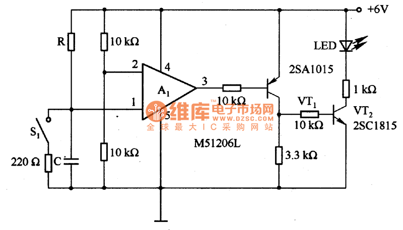
The time delay circuit diagram composed of transistor
The circuit is designed to set a delay time based on the voltage Us and the resistor R. In this configuration, S1 acts as the discharge switch for capacitor C. When switch S1 is closed, the stored charge in capacitor...

1 Transistor Toggle Relay schematic
The circuit below requires a double pole, double throw relay in conjunction with a single transistor to allow toggling the relay with a momentary push button. One set of relay contacts is used to control the load, while the other...

All transistor microphone pre-amplifier
The microphone has high sensitivity in the audio range, but in the ultrasonic range, the sensitivity decreases rapidly. The receiver is very sensitive. To prevent overdriving and feedback due to the high sensitivity of the microphone in the audio range,...

improved 3 transistor audio amp
This circuit is similar to the previous one but employs positive feedback to enhance the amplitude delivered to the speaker. It is adapted from a small 5-transistor radio that utilizes a 25-ohm speaker. In the earlier circuit, the load resistor...

TRANSISTOR MOTOR CONTROLLER
Despite the high impedance of its inputs, the Darlington transistor Q10 generates sufficient current to drive an LED. The inverted output of Q10 powers the internal LED of opto isolator U5, which, in turn, couples to the motor control triac...
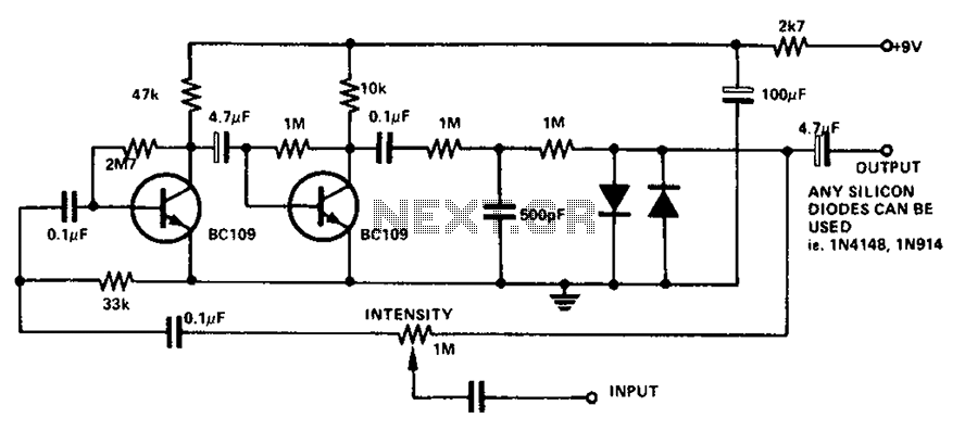
Boombox circuit diagram
The circuit utilizes a transistor to amplify the input signal. Two diodes are employed to clamp the distorted output, while a 500 pF capacitor filters out high-frequency noise. Under normal conditions, a 1M slide rheostat is used to adjust the...

Kapanadze 5
The emitter voltage drops completely to 0V from 42V during the pulse when the transistor is conducting or saturated. This contrasts with a pure resistive load (the 4.7 Ohm resistor mentioned in the previous video), where the collector-emitter voltage does...