


Simple Battery Charger using LM350
#LM350
#constant voltage
#temperature coefficient
#transistor
#BD140
#voltage regulator
#battery protection
#charging circuit
#power management
#negative temperature coefficient

Description: The circuit is designed as a constant voltage source with a negative temperature coefficient. The transistor Q1 (BD 140) serves as the temperature sensor, while transistor Q2 prevents battery discharge through resistor R1 when mains power is unavailable. The circuit utilizes the voltage regulator IC LM350, allowing the output voltage of the charger to be adjusted between 13-15 V by varying the potentiometer R6. The LM350 maintains a constant voltage drop of 1.25 V between its input and output pins, ensuring a steady current flow through resistor R1. Q1 functions as a temperature sensor, aided by components R6, R3, and R4, which regulate the base current of Q1. The emitter/base connection of transistor Q1 exhibits a temperature coefficient of -2 mV/°C, resulting in a negative temperature coefficient for the output voltage approximately four times larger, leading to around -8 mV/°C due to the interaction of the emitter/base of Q1 and the division factor of P1, R3, and R4. An LED indicator illuminates whenever mains power is available.
The circuit operates effectively as a constant voltage source, utilizing the LM350 voltage regulator, which is known for its ability to maintain a stable output voltage under varying load conditions. The LM350 is configured to provide an output voltage that can be finely tuned between 13 V and 15 V through the use of potentiometer R6, allowing for customization based on specific application requirements.
Transistor Q1 (BD 140) plays a crucial role in temperature compensation; it acts as a temperature sensor that responds to changes in ambient temperature. The negative temperature coefficient of the output voltage is a result of the inherent characteristics of Q1, which decreases in voltage with increasing temperature. This is further amplified by the circuit configuration involving resistors R3 and R4, which influence the base current and, consequently, the behavior of Q1.
Transistor Q2 functions as a switch that ensures the battery does not discharge through resistor R1 when the mains power is not present, thereby protecting the battery and extending its life. The LED indicator provides a visual cue that mains power is available, enhancing the usability of the circuit.
Overall, this design effectively combines temperature compensation with voltage regulation, making it suitable for applications where stable voltage output is critical in varying temperature environments. The careful selection of components and their configuration allows for precise control over both the output voltage and the thermal behavior of the circuit.The circuit is designed as a constant voltage source with a negative temperature coefficient. The transistor Q1 (BD 140) is used as the temperature sensor. The transistor Q2 is used to prevent the battery from discharging through R1 when the mains power is not available. The circuit is designed based on the voltage regulator IC LM350. The output voltage of the charger can be adjusted between 13-15 V by varying the POT R6. The LM350 will try to keep the voltage drop between its input pin and the output pin at a constant value of 1. 25V. So there will be a constant current flow through the resistor R1. Q1 act here as a temperature sensors with the help of components R6/R3/R4 which more or less control the base current of Q1.
As the emitter/base connection of transitor Q1, just like any other semiconductor, contains a temperature coefficient of -2mV/ °C, the output voltage will also show a negative temperature coefficient. That one is only a factor of 4 larger, because of the variation of the emitter/basis of Q1 multiplied by the division factor of P1/R3/R4.
This results in approximately -8mV/ °C. The LED will glow whenever the mains power is available.
The circuit operates effectively as a constant voltage source, utilizing the LM350 voltage regulator, which is known for its ability to maintain a stable output voltage under varying load conditions. The LM350 is configured to provide an output voltage that can be finely tuned between 13 V and 15 V through the use of potentiometer R6, allowing for customization based on specific application requirements.
Transistor Q1 (BD 140) plays a crucial role in temperature compensation; it acts as a temperature sensor that responds to changes in ambient temperature. The negative temperature coefficient of the output voltage is a result of the inherent characteristics of Q1, which decreases in voltage with increasing temperature. This is further amplified by the circuit configuration involving resistors R3 and R4, which influence the base current and, consequently, the behavior of Q1.
Transistor Q2 functions as a switch that ensures the battery does not discharge through resistor R1 when the mains power is not present, thereby protecting the battery and extending its life. The LED indicator provides a visual cue that mains power is available, enhancing the usability of the circuit.
Overall, this design effectively combines temperature compensation with voltage regulation, making it suitable for applications where stable voltage output is critical in varying temperature environments. The careful selection of components and their configuration allows for precise control over both the output voltage and the thermal behavior of the circuit.The circuit is designed as a constant voltage source with a negative temperature coefficient. The transistor Q1 (BD 140) is used as the temperature sensor. The transistor Q2 is used to prevent the battery from discharging through R1 when the mains power is not available. The circuit is designed based on the voltage regulator IC LM350. The output voltage of the charger can be adjusted between 13-15 V by varying the POT R6. The LM350 will try to keep the voltage drop between its input pin and the output pin at a constant value of 1. 25V. So there will be a constant current flow through the resistor R1. Q1 act here as a temperature sensors with the help of components R6/R3/R4 which more or less control the base current of Q1.
As the emitter/base connection of transitor Q1, just like any other semiconductor, contains a temperature coefficient of -2mV/ °C, the output voltage will also show a negative temperature coefficient. That one is only a factor of 4 larger, because of the variation of the emitter/basis of Q1 multiplied by the division factor of P1/R3/R4.
This results in approximately -8mV/ °C. The LED will glow whenever the mains power is available.

ECM Mic Preamplifier
Both transistors should be low-noise types. In the original circuit, BC650C was used, which is an ultra-low noise device. These transistors are now difficult to find, but BC549C or BC109C are good replacements. The circuit is self-stabilizing and will set...

Transistor Tutorial Power Amplifiers Part 4
An audio power amplifier can enhance weak signals from devices like tuners, CD players, or tape decks to fill a room with sound. This article emphasizes the operating principles and circuitry of low-frequency power amplifiers utilizing bipolar junction transistors (BJTs)....

Simple Short Finder Circuit
Transistors Q1 and Q2, along with resistors R1 through R7, form the input balancing stage that measures the resistance between points X and Y. This stage operates as a bridge circuit, incorporating resistors R1, R2, R6, R7, and the resistance...

Positive-regulator-with-pnp-boost
The IC8211 serves as the voltage reference and regulator amplifier, with Q1 functioning as the series pass transistor. Resistor R1 defines the output current of the IC8211, while capacitors C1 and C2 ensure loop stability and help suppress the feedthrough...

Single-junction transistor trigger circuit 2
Due to the increased level of the transistor amplifier circuit, the control circuit's performance in Figure 16-6 is more sensitive and can accept input control signals superimposed on others (such as voltage, current, and speed feedback signals) to meet system...

Common emitter amplifier input and output signals of the phase relationship
The common emitter amplifier circuit exhibits a specific phase relationship between its input and output signals. This configuration is widely utilized in various electronic devices primarily for its high voltage gain. However, the output impedance is higher than the input...
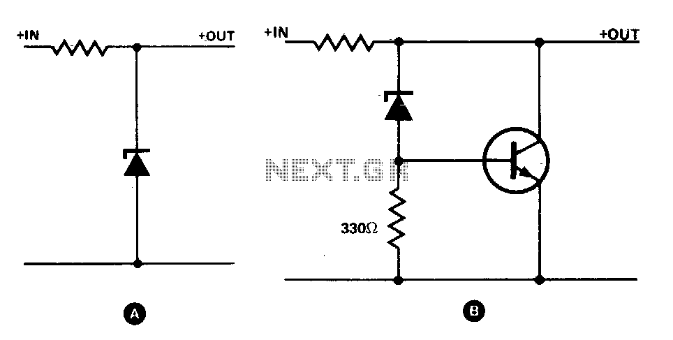
Transistor increases zener rating
The simple zener shunt in configuration A may not handle sufficient current if the zener diode available is of low wattage. A power transistor will perform most of the work for the zener as illustrated in configuration B. Once the...

Basic reference bias circuit transistor - negative voltage feedback
Basic reference bias circuit using a transistor with negative voltage feedback.
The basic reference bias circuit utilizing a transistor with negative voltage feedback is designed to provide a stable output voltage or current that is largely independent of variations in temperature...

Symmetric Noise Source
When a transistor junction operates in Zener breakdown as a noise source, the resulting noise signal exhibits asymmetry in amplitude. This issue can be addressed by employing two transistors as independent noise sources. One transistor is connected with a series...