


Supercapacitor charger electronic circuit using LTC3625
#supercapacitor
#LTC3625
#voltage regulator
#cell balancing
#energy storage
#power management
#Linear technology
#electronic circuit
#charging circuit
#fixed output voltage

Description: A simple supercapacitor charger electronic project can be designed using the LTC3625 integrated circuit (IC) from Linear Technology. This circuit is capable of charging two supercapacitors in series to a fixed output voltage of either 4.8V/5.3V or 4V/4.5V, which can be selected based on the application. The input supply range for this project is from 2.7V to 5.5V. The LTC3625 features automatic cell balancing, which prevents overvoltage damage to either supercapacitor while maximizing the charge rate without the need for balancing resistors. The circuit diagram demonstrates high efficiency, high charging current, low quiescent current, and requires minimal external components. The charging current and maximum input current level can be programmed using an external resistor. When the input supply is disconnected or the EN pin is set low, the LTC3625 automatically enters a low current state, drawing less than 1 µA. This circuit is straightforward, requiring only a few external electronic components in addition to the LTC3625 IC and a solar panel, including an LT1784 operational amplifier and some common external parts.
The LTC3625 is a high-performance buck-boost converter designed specifically for supercapacitor charging applications. Its ability to operate over a wide input voltage range makes it suitable for various power sources, including batteries and solar panels. The device's efficiency is critical, as it ensures that most of the input power is converted into usable output energy, minimizing losses during the charging process. The fixed output voltage selection allows for flexibility in applications, enabling the user to adapt the circuit to different supercapacitor configurations.
The automatic cell balancing feature of the LTC3625 is particularly advantageous, as it ensures that both supercapacitors charge equally, thus extending their lifespan and maintaining performance. This is achieved without the need for external balancing resistors, which can introduce additional complexity and power loss. Instead, the LTC3625 internally manages the balancing process, allowing for a more compact and efficient design.
The choice of an LT1784 operational amplifier in this circuit further enhances performance. The LT1784 is known for its low offset voltage and low noise characteristics, making it ideal for precision applications where accurate voltage levels are crucial. This op-amp can be used in feedback loops or signal conditioning stages within the circuit, contributing to the overall stability and reliability of the supercapacitor charging process.
Overall, this supercapacitor charger circuit is a robust solution for energy storage applications, combining high efficiency, ease of use, and minimal component requirements. The design is particularly suited for renewable energy applications, such as solar energy systems, where effective energy storage is essential for continuous power supply. The simplicity of the circuit allows for easy integration into various projects, making it an excellent choice for both hobbyists and professionals in the field of electronics.A very simple supercapacitor charger electronic project can be designed using the LTC3625 IC designed by Linear technology to charge two supercapacitors in series to a fixed output voltage (4. 8V/5. 3V or 4V/4. 5V selectable) from a 2. 7V to 5. 5V input supply. Automatic cell balancing prevents overvoltage damage to either supercapacitor while maximizi ng charge rate without using any balancing resistors. This electronic circuit project presented in this circuit diagram has high efficiency, high charging current, low quiescent current and require low minimum external parts Charging current/maximum input current level is programmed with an external resistor. When the input supply is removed and/or the EN pin is low, the LTC3625 automatically enter a low current state, drawing less than 1 A.
The circuit is very simple requiring few external electronic parts, excepting the LTC3625 IC and solar panel this circuit project require a LT1784 op amp and some common external parts.
The LTC3625 is a high-performance buck-boost converter designed specifically for supercapacitor charging applications. Its ability to operate over a wide input voltage range makes it suitable for various power sources, including batteries and solar panels. The device's efficiency is critical, as it ensures that most of the input power is converted into usable output energy, minimizing losses during the charging process. The fixed output voltage selection allows for flexibility in applications, enabling the user to adapt the circuit to different supercapacitor configurations.
The automatic cell balancing feature of the LTC3625 is particularly advantageous, as it ensures that both supercapacitors charge equally, thus extending their lifespan and maintaining performance. This is achieved without the need for external balancing resistors, which can introduce additional complexity and power loss. Instead, the LTC3625 internally manages the balancing process, allowing for a more compact and efficient design.
The choice of an LT1784 operational amplifier in this circuit further enhances performance. The LT1784 is known for its low offset voltage and low noise characteristics, making it ideal for precision applications where accurate voltage levels are crucial. This op-amp can be used in feedback loops or signal conditioning stages within the circuit, contributing to the overall stability and reliability of the supercapacitor charging process.
Overall, this supercapacitor charger circuit is a robust solution for energy storage applications, combining high efficiency, ease of use, and minimal component requirements. The design is particularly suited for renewable energy applications, such as solar energy systems, where effective energy storage is essential for continuous power supply. The simplicity of the circuit allows for easy integration into various projects, making it an excellent choice for both hobbyists and professionals in the field of electronics.A very simple supercapacitor charger electronic project can be designed using the LTC3625 IC designed by Linear technology to charge two supercapacitors in series to a fixed output voltage (4. 8V/5. 3V or 4V/4. 5V selectable) from a 2. 7V to 5. 5V input supply. Automatic cell balancing prevents overvoltage damage to either supercapacitor while maximizi ng charge rate without using any balancing resistors. This electronic circuit project presented in this circuit diagram has high efficiency, high charging current, low quiescent current and require low minimum external parts Charging current/maximum input current level is programmed with an external resistor. When the input supply is removed and/or the EN pin is low, the LTC3625 automatically enter a low current state, drawing less than 1 A.
The circuit is very simple requiring few external electronic parts, excepting the LTC3625 IC and solar panel this circuit project require a LT1784 op amp and some common external parts.

LM7805 + 5V power supply configuration
The circuit illustrated in the figure provides an output voltage of +5V and an output current of 1.5A. It comprises a power transformer, a bridge rectifier circuit consisting of diodes D1 to D4, and filter capacitor C1. Additionally, capacitors C2...

2.5V voltage regulator circuit
A 2.5V voltage regulator circuit is illustrated, which is part of a computer's motherboard. The circuit employs an oscillation circuit with the RT9202 control core chip, converting a 5V input supply into a regulated +2.5V output voltage, with the chip's...

BMW R Series Motorcycle Regulator Schematic
Correctly adjusted, the voltage on the pot wiper is slightly less than half D+ (appx. 0.47*D+) and Q1 will conduct if (D+)-(Vp) > 6.2 + 0.7 + 0.7, or 0.53*(D+) > 7.6V, (D+) > 14.3V. If D+ is lower than...

0-50V 1A power supply with CA3086
This power supply circuit is highly stabilized that its output voltage will drop only 0.005% even though the load changes from 0 to 100%. Another excellent capability is that the output voltage will change only by 0.01% if the input...

Temperature compensation of the symmetrical power supply 7812 F007C
The circuit is a temperature-compensated power supply that generates a negative voltage to track positive voltage changes in a symmetrical voltage integrated power supply. It features a three-terminal regulator connected with two identical transistors, leveraging the temperature characteristics of the...

Voltage Regulator
This regulator is suitable for devices that need up to 1mA. For higher output current, the resistors would have to be scaled down in reverse proportion to the peak current expected. With the resistor values shown, the regulator draws a...

avr case
Bruco Integrated Circuits B.V. - Case: Automotive alternator voltage regulator - Bruco.
The automotive alternator voltage regulator designed by Bruco Integrated Circuits B.V. is a critical component in modern vehicle electrical systems. This device is responsible for regulating the voltage output...
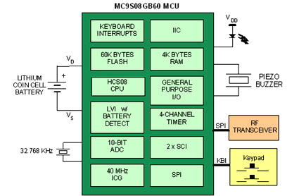
How to extend the battery life of your microcontroller based design
Battery-powered devices, such as electric toothbrushes, shavers, cell phones, PDAs, MP3 players, and remote controls, are integral to daily life. Consequently, power management has become a critical consideration for embedded designers. Microcontrollers (MCUs) provide various methods for managing power requirements...

Micropower Linear Voltage Regulator in the Battery Charger Circuit
The ADM666A application note provides a detailed explanation of a low-cost battery charger circuit, including maximum output voltage, charge termination voltage calculation, battery voltage level monitoring, and circuit efficiency optimization. The ADM666A utilizes an NPN transistor and a P-channel FET....