


AD8195 and DDC buffers

Description: The DDC lines on the HDMI connector side have a pull-up resistor of 47 kOhms connected to 5V and a 2 kOhm pull-up resistor connected to 3.3V on the FPGA side. The schematic indicates that the glitch is a normal part of the operation of the DDC buffer in the AD8195. This glitch occurs only on the rising edge of the transmitting side of the DDC transaction and should not negatively impact the receiving device. Additional inquiries include identifying the source device, the SCL frequency, and whether failures occur during reads, writes, or both. A view of the failing DDC transaction on both the input and output of the AD8195 is also requested.
The HDMI DDC (Display Data Channel) lines are critical for communication between the source device and the display. The pull-up resistors integrated into the circuit design ensure that the DDC lines maintain appropriate voltage levels, facilitating reliable data transmission. The 47 kOhm pull-up resistor connected to the 5V supply on the HDMI connector side serves to pull the DDC lines high when they are not being actively driven low, ensuring that the logic level remains stable. On the FPGA side, the 2 kOhm pull-up resistor connected to the 3.3V supply provides a compatible voltage level for the FPGA's input requirements.
The AD8195, a high-speed HDMI switch, incorporates a DDC buffer that manages the DDC communication. The noted glitch occurring during the rising edge of the DDC transaction is a common phenomenon in digital circuits, particularly in high-speed environments. This glitch is typically a result of signal integrity issues, such as capacitance or inductance in the circuit, but it is designed not to interfere with the overall data integrity of the DDC transactions. The receiving device is expected to recognize valid data despite this transient glitch, as it is momentary and does not persist long enough to corrupt the data being transmitted.
Further investigation into the read/write errors may involve analyzing the SCL frequency, which dictates the speed of the I2C communication over the DDC lines. Identifying the source device can help determine if there are compatibility issues or if the device's configuration is contributing to the observed errors. Additionally, understanding whether failures occur during reads, writes, or both can assist in pinpointing the exact nature of the problem. A detailed examination of the DDC transaction signals on both the input and output sides of the AD8195 would provide valuable insights into the operational status and help diagnose the underlying issue more effectively.The DDC lines on HDMI connector side are 47KOhms 5V PU and 2KOhms 3. 3V PU on FPGA side. Our schematic look like this one: This glitch is part of the normal operation of the DDC buffer in the AD8195. The glitch only occurs on the rising edge of the transmitting side of the DDC transaction and therefore should not adversely affect the receiving device.
Perhaps there is another issue causing the read/write errors. I`ll be happy to help diagnose the issue. What is the source device What is SCL frequency Do failures occur during reads or writes or both Can you provide a view of the failing DDC transaction both on input and output of AD8195
The HDMI DDC (Display Data Channel) lines are critical for communication between the source device and the display. The pull-up resistors integrated into the circuit design ensure that the DDC lines maintain appropriate voltage levels, facilitating reliable data transmission. The 47 kOhm pull-up resistor connected to the 5V supply on the HDMI connector side serves to pull the DDC lines high when they are not being actively driven low, ensuring that the logic level remains stable. On the FPGA side, the 2 kOhm pull-up resistor connected to the 3.3V supply provides a compatible voltage level for the FPGA's input requirements.
The AD8195, a high-speed HDMI switch, incorporates a DDC buffer that manages the DDC communication. The noted glitch occurring during the rising edge of the DDC transaction is a common phenomenon in digital circuits, particularly in high-speed environments. This glitch is typically a result of signal integrity issues, such as capacitance or inductance in the circuit, but it is designed not to interfere with the overall data integrity of the DDC transactions. The receiving device is expected to recognize valid data despite this transient glitch, as it is momentary and does not persist long enough to corrupt the data being transmitted.
Further investigation into the read/write errors may involve analyzing the SCL frequency, which dictates the speed of the I2C communication over the DDC lines. Identifying the source device can help determine if there are compatibility issues or if the device's configuration is contributing to the observed errors. Additionally, understanding whether failures occur during reads, writes, or both can assist in pinpointing the exact nature of the problem. A detailed examination of the DDC transaction signals on both the input and output sides of the AD8195 would provide valuable insights into the operational status and help diagnose the underlying issue more effectively.The DDC lines on HDMI connector side are 47KOhms 5V PU and 2KOhms 3. 3V PU on FPGA side. Our schematic look like this one: This glitch is part of the normal operation of the DDC buffer in the AD8195. The glitch only occurs on the rising edge of the transmitting side of the DDC transaction and therefore should not adversely affect the receiving device.
Perhaps there is another issue causing the read/write errors. I`ll be happy to help diagnose the issue. What is the source device What is SCL frequency Do failures occur during reads or writes or both Can you provide a view of the failing DDC transaction both on input and output of AD8195

FPGA RS232 Serial Interface Circuit
The schematic for this project is a modified version of the CPLD development board schematic. Several new components have been added for this project, and the completed schematic can be viewed below. The main components in the schematic are the...

LEDs and Switches
The DE2 board features four pushbutton switches, each of which is debounced using a Schmitt Trigger circuit, as shown in Figure 1. The outputs, labeled KEY0 to KEY3, from the Schmitt Trigger are directly connected to the Cyclone II FPGA....

5V Power Supply For On-Train Radio Camera
A radio camera on a model railway should transmit constantly while the train is moving and continue transmitting for a few minutes after the train stops.
The design of a radio camera system for a model railway requires careful consideration to...

development and evaluation for FPGA based systems
The System Monitor feature discussed in this article was successfully utilized by Avalon Microelectronics in two Virtex-5 FPGAs (XC5VLX330T) during their development. They encountered an unusual issue where the development board would shut down while the FPGAs were executing certain...
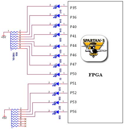
traffic light interfacing with spartan 3 primer
The Spartan-3 board features a traffic light controller utilizing FPGA I/O pins. The traffic light controller card consists of 12 point LEDs arranged in 4 lanes. Each lane is equipped with three LEDs: Go (Green), Listen (Yellow), and Stop (Red)....

2 transistor buffer
When designed with general-purpose small-signal transistors, the bandwidth ranges from 50 MHz to 250 MHz, necessitating careful grounding and power supply decoupling. The simulation schematic illustrates a two-transistor buffer. Due to copyright issues, models from other sources are not included...

5V 0.5A power supply
The circuit functions as a constant voltage source, modified by feedback components R2 and R3 to maintain a stable output voltage. The ZN424E output must be at least 2 volts above the negative rail, with the load connected to the...
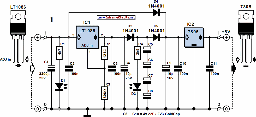
5V Power Supply For On-Train Radio Camera
A radio camera on a model railway is designed to transmit continuously while the train is in motion and to keep transmitting for a few minutes after the train comes to a stop. If the train resumes movement after a...

How to design 65nm FPGA DDR2 memory
This article discusses practical techniques for incorporating "correctness by design" in DDR2 interfaces from a Signal Integrity (SI) perspective, utilizing the current generation of available design tools. It analyzes common DDR2 design errors and the trade-offs between various popular design...