


Fiber-optic-transmitter
#fiber-optic
#LED driver
#74F3040
#NE592
#NE564
#NE522
#video signal
#sync tip clamp
#wideband differential amplifier

Description: An alternate LED driver utilizing the 74F3040 line driver has been implemented in this application example. The 74F3040 offers a higher current rating but lacks the variable threshold capabilities found in the NE522. The LED diode operates in a saturated on-off mode to achieve optimal signal-to-noise performance. This receiver circuit comprises a wideband differential amplifier (NE592), a voltage-controlled oscillator (VCO) (NE564), and an LED driver (NE522), which functions as a high-speed comparator. The video signal is AC coupled into the modulator preamplifier, followed by a sync tip clamp that restores the composite video signal and prevents modulation deviation variations with changing picture content. A video signal level of 250 to 300 mV peak is necessary to maintain optimal picture modulation. Frequency compensation (preemphasis) is introduced through a passive RC lead network at the input of the NE592 differential amplifier. The main FM modulator consists of the NE564, which is employed solely as a linear wideband VCO, while the other sections of the device remain unused. Differential decoupling to the VCO terminals is achieved via the loop filter terminals, specifically pins 4 and 5.
The circuit design incorporates a robust LED driver configuration using the 74F3040 to enhance current handling capabilities. This choice is particularly suitable for applications requiring high drive strength, despite the absence of variable threshold functionality. Operating the LED diode in a saturated on-off mode ensures maximum signal clarity and minimizes noise interference, which is critical for high-fidelity signal transmission.
The NE592 wideband differential amplifier plays a pivotal role in signal processing, providing the necessary gain and bandwidth to accommodate the video signal requirements. By utilizing AC coupling, the circuit effectively eliminates DC offsets, ensuring that the video signal remains centered around zero volts, which is essential for proper modulation. The inclusion of a sync tip clamp further stabilizes the composite video signal, mitigating variations in modulation deviation that can arise from dynamic changes in picture content.
To maintain optimal picture modulation, a specific input video signal level of 250 to 300 mV peak is essential. This requirement is crucial for ensuring that the modulation index remains within the desired range, thereby preserving the integrity of the transmitted image. The frequency compensation implemented through a passive RC network at the NE592 input serves to enhance transient response and reduce distortion, ensuring that the amplifier can accurately reproduce fast-changing video signals.
The NE564 serves as the primary FM modulator in this configuration, functioning exclusively as a linear wideband VCO. This approach allows for precise frequency modulation of the input signal while ensuring that the other sections of the device are not utilized, simplifying the design and improving reliability. The differential decoupling to the VCO terminals through the loop filter terminals (pins 4 and 5) ensures stable operation and minimizes noise coupling, further enhancing the performance of the overall circuit. This careful consideration of component selection and configuration results in a highly effective LED driver and video modulation system.An alternate LED driver which uses the 74F3040 line driver was incorporated in this particular application example. The 74F3040.has a higher current rating, but not the variable threshold capabilities at the NE522. The LED diode is operated in the saturated on-off mode for best signal to noise. This receiver circuit consists of wideband differential amplifier NE592, VCO NE564 and LED driver NE522-tbe high-speed comparator.
The video signal is ac coupled into the modulator preamplifier and followed by a sync tip clamp to provide de restoration on the composite video signal and to prevent variation of modulation deviation with varying picture content. A video signal level of 250 to 300 m V peak is required to maintain optimnm picture modulation. Frequency compensation (preemphasis) is inserted in the form of a passive rc lead network at tbe input to the NE592 differential amplifier. The main FM modulator consists of an NE564 used only as a linear wideband VCO, but the other sections of the device are not used.
Differential de coupling to tbe VCO terminals is attained via tbe loop filter terminals, pins 4 and 5.
The circuit design incorporates a robust LED driver configuration using the 74F3040 to enhance current handling capabilities. This choice is particularly suitable for applications requiring high drive strength, despite the absence of variable threshold functionality. Operating the LED diode in a saturated on-off mode ensures maximum signal clarity and minimizes noise interference, which is critical for high-fidelity signal transmission.
The NE592 wideband differential amplifier plays a pivotal role in signal processing, providing the necessary gain and bandwidth to accommodate the video signal requirements. By utilizing AC coupling, the circuit effectively eliminates DC offsets, ensuring that the video signal remains centered around zero volts, which is essential for proper modulation. The inclusion of a sync tip clamp further stabilizes the composite video signal, mitigating variations in modulation deviation that can arise from dynamic changes in picture content.
To maintain optimal picture modulation, a specific input video signal level of 250 to 300 mV peak is essential. This requirement is crucial for ensuring that the modulation index remains within the desired range, thereby preserving the integrity of the transmitted image. The frequency compensation implemented through a passive RC network at the NE592 input serves to enhance transient response and reduce distortion, ensuring that the amplifier can accurately reproduce fast-changing video signals.
The NE564 serves as the primary FM modulator in this configuration, functioning exclusively as a linear wideband VCO. This approach allows for precise frequency modulation of the input signal while ensuring that the other sections of the device are not utilized, simplifying the design and improving reliability. The differential decoupling to the VCO terminals through the loop filter terminals (pins 4 and 5) ensures stable operation and minimizes noise coupling, further enhancing the performance of the overall circuit. This careful consideration of component selection and configuration results in a highly effective LED driver and video modulation system.An alternate LED driver which uses the 74F3040 line driver was incorporated in this particular application example. The 74F3040.has a higher current rating, but not the variable threshold capabilities at the NE522. The LED diode is operated in the saturated on-off mode for best signal to noise. This receiver circuit consists of wideband differential amplifier NE592, VCO NE564 and LED driver NE522-tbe high-speed comparator.
The video signal is ac coupled into the modulator preamplifier and followed by a sync tip clamp to provide de restoration on the composite video signal and to prevent variation of modulation deviation with varying picture content. A video signal level of 250 to 300 m V peak is required to maintain optimnm picture modulation. Frequency compensation (preemphasis) is inserted in the form of a passive rc lead network at tbe input to the NE592 differential amplifier. The main FM modulator consists of an NE564 used only as a linear wideband VCO, but the other sections of the device are not used.
Differential de coupling to tbe VCO terminals is attained via tbe loop filter terminals, pins 4 and 5.

Automotive LED driver circuit diagram LT3486
The automotive LED driver circuit diagram utilizes the LT3486. The LED is employed in the car's central high-mounted stop lamp (CHMSL), providing advantages such as faster achievement of the set brightness, higher efficiency, longer lifespan, and simplified design and installation...
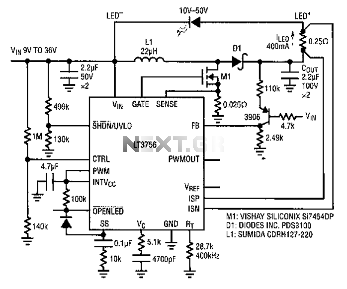
Based LT3756 buck - boost mode drive circuit diagram
Common LED driver requirements include a wide and overlapping range of LED string voltages and input voltages. Many designers prefer to use an LED driver circuit that accommodates various battery power sources and multiple LED strings. This universal configuration may...

MAX7316 white LED driver circuit diagram
The main technical characteristics of the MAX7316 include a 400 kbps, 2-wire serial interface with a voltage tolerance of 5.5V. The operating voltage ranges from 2V to 3.6V. It features 8-bit PWM control for white LED brightness, with global brightness...

LED-Driver Design for Automotive Rear Lighting
This article discusses the design of an LED driver for automotive rear lights. It demonstrates that dimming is most effectively accomplished using pulse-width modulation (PWM) in conjunction with an LED driver integrated circuit (IC) that removes the requirement for an...

Power Driver For 20W LED circuit
This lighting solution offers over 90% energy savings compared to incandescent or halogen bulbs, with a lifespan exceeding 50,000 hours. It operates without flickering, making it suitable for human eyes, and produces no RF interference or UV radiation. The design...

A High Power Led Driver For Low Voltage Halogen Replacement
Application of the High Power LED Driver SP7652 with an Analog 0V-to-10V dimmer. Electrical Requirements: Input Voltage of 5.5V to 28V, Output Voltage VF of LED, Output Current ranging from 0 to 6A. This circuit is designed to provide a...

Blue White LED Driver Circuit Joule Thief
This post discusses blue and white LED drivers utilizing a joule thief circuit. Further exploration of the circuit's functionality is provided, along with simulation points.
The joule thief circuit is a simple and efficient boost converter that allows for the operation...
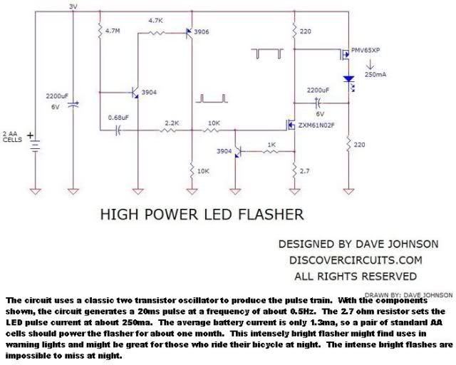
Random oscillator circuit for high power LEDs
A circuit is needed to drive three or more LEDs at a current of 200-350mA each, with the capability to randomly flash or strobe them at a frequency of 5-20Hz. The input power should be low-voltage DC, with a preference...

TA7366 67 five lights single drive circuit
The TA 7366/7367 is a commonly used single display driver circuit manufactured by Toshiba Corporation. It features a 5 LED driver circuit and is designed in a 9-pin single in-line plastic structure. The circuit configuration includes an operational amplifier (op-amp)...