


Build A Byte Blaster Circuit

Description: This schematic is directly sourced from the Altera ByteBlaster datasheet or manual, which provides comprehensive details regarding the connector's functionality and pin connections. It is advisable to review the datasheet available on their website or through a search engine for thorough understanding. The 74LS244 is a Low Power Schottky Octal Buffer. A limitation of this design is that some computer parallel ports may not supply sufficient power for this circuit. The ByteBlaster MV is an updated design that addresses this issue, which will be discussed further. The resistors in this design serve as simple current-limiting components, ensuring that no surge of current from the JTAG or parallel ports can potentially damage the 74LS244. The pins for the 10-pin connector are clearly labeled, with only 8 out of the 10 pins connected to the JTAG-style connector.
The schematic in question is integral to understanding the operation of the Altera ByteBlaster, a device used for programming and debugging FPGA and CPLD devices. The 74LS244 octal buffer plays a crucial role in this circuit, providing signal buffering and isolation between the programming interface and the target device. This is particularly important to maintain signal integrity and protect sensitive components from potential damage due to high current levels.
In this design, the use of current-limiting resistors is essential. These resistors are strategically placed to prevent excessive current flow that could occur during signal transitions, which could otherwise lead to overheating or failure of the 74LS244. The careful selection of these resistors ensures that the circuit operates within safe limits, allowing for reliable performance across varying conditions.
The 10-pin connector is a critical interface for the ByteBlaster, enabling communication between the programming device and the target hardware. Although the connector features 10 pins, only 8 are utilized in the JTAG configuration. This pin arrangement is designed to facilitate straightforward connections while minimizing the risk of miswiring. Each pin's function is labeled clearly, aiding in the assembly and troubleshooting processes.
The updated ByteBlaster MV design provides enhancements over the original model, particularly in power management. By addressing the power limitations of some parallel ports, it ensures that the device can operate effectively across a wider range of systems. This advancement is vital for users who require compatibility with various computer architectures and configurations.
In summary, the schematic derived from the Altera ByteBlaster documentation encapsulates essential design elements, including the role of the 74LS244 buffer, the importance of current-limiting resistors, and the functionality of the 10-pin connector. Understanding these components is crucial for effective implementation and operation of the ByteBlaster in programming and debugging applications.This schematic is taken directly from the Altera ByteBlaster datasheet or manual. They spill out all the fine print and details of how the connector works & what connections go where. Find the datasheet on their website or through google and give it a good read through. The 74LS244 is a Low Power Schottky Octal Buffer. A downside to using this ch ip in this design is that some computer parallel ports may not offer enough power for this circuit. The ByteBlaster MV is an updated design that solves this problem, something we`ll explore later on. These resisitors act as simple current limiting resistors. They make sure no surge of current can come from the JTAG or Parallel ports that might potentially damage the 74LS244. The pins for the 10-Pin connector are again clearly labeled. Notice that only 8 of the 10 pins are actually connected to the JTAG style connector.
The schematic in question is integral to understanding the operation of the Altera ByteBlaster, a device used for programming and debugging FPGA and CPLD devices. The 74LS244 octal buffer plays a crucial role in this circuit, providing signal buffering and isolation between the programming interface and the target device. This is particularly important to maintain signal integrity and protect sensitive components from potential damage due to high current levels.
In this design, the use of current-limiting resistors is essential. These resistors are strategically placed to prevent excessive current flow that could occur during signal transitions, which could otherwise lead to overheating or failure of the 74LS244. The careful selection of these resistors ensures that the circuit operates within safe limits, allowing for reliable performance across varying conditions.
The 10-pin connector is a critical interface for the ByteBlaster, enabling communication between the programming device and the target hardware. Although the connector features 10 pins, only 8 are utilized in the JTAG configuration. This pin arrangement is designed to facilitate straightforward connections while minimizing the risk of miswiring. Each pin's function is labeled clearly, aiding in the assembly and troubleshooting processes.
The updated ByteBlaster MV design provides enhancements over the original model, particularly in power management. By addressing the power limitations of some parallel ports, it ensures that the device can operate effectively across a wider range of systems. This advancement is vital for users who require compatibility with various computer architectures and configurations.
In summary, the schematic derived from the Altera ByteBlaster documentation encapsulates essential design elements, including the role of the 74LS244 buffer, the importance of current-limiting resistors, and the functionality of the 10-pin connector. Understanding these components is crucial for effective implementation and operation of the ByteBlaster in programming and debugging applications.This schematic is taken directly from the Altera ByteBlaster datasheet or manual. They spill out all the fine print and details of how the connector works & what connections go where. Find the datasheet on their website or through google and give it a good read through. The 74LS244 is a Low Power Schottky Octal Buffer. A downside to using this ch ip in this design is that some computer parallel ports may not offer enough power for this circuit. The ByteBlaster MV is an updated design that solves this problem, something we`ll explore later on. These resisitors act as simple current limiting resistors. They make sure no surge of current can come from the JTAG or Parallel ports that might potentially damage the 74LS244. The pins for the 10-Pin connector are again clearly labeled. Notice that only 8 of the 10 pins are actually connected to the JTAG style connector.
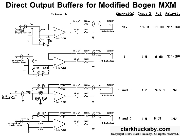
Implementation of Direct Output Buffers
A total of six buffer circuits utilizing three dual op-amp packages are implemented, with five designated for input channels and one for the master output channel. These circuits feature high input impedance, particularly for the five buffers interfacing with channel...

circuit schematic symbol for buffer with control input
Circuit 1kZ incorporates an operational amplifier (op-amp) component with two inputs, one output, and up and down ports, typically utilized for power supply rails. Additionally, there is a buffer component, which is likely provided by TikZ itself rather than the...

Buffer Circuit Schematic Diagram
The series consists of input buffers that match the output. This configuration resembles a common collector circuit with a reinforcement factor of 1. A resistor value is included to limit the current usage. The effectiveness of this circuit largely depends...
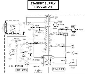
Need to have the circuit schematic for LG 29SA1RL model
The schematic is in PDF format and cannot be sent through this site. It is recommended to check a specific website that contains various schematics, including older posts that might have the schematic needed. A WS-55807 model is experiencing issues...
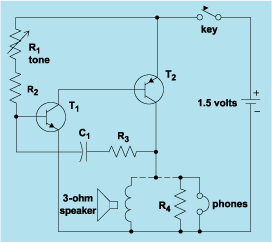
schematic diagram graphic arts
Schematic diagram. A presentation of the element-by-element relationship of all parts of a system.
A schematic diagram serves as a crucial tool in electronic design and engineering, representing the interconnections and relationships between various components within a system. It provides a...

Aladin
Whoever thinks about reproducing an interface for the Aladin should first of all be aware of the fact that there are two different versions of the interface. The first version, easier to assemble, enables the user to transfer dive data...

avr What is the point of Buffers like this in Programmers
At the bottom, there is a 74AC125, which is a quad buffer with tri-state outputs. Numerous buffers of this type have been observed in programmers. The function of these buffers is not entirely clear, but it is assumed that the...
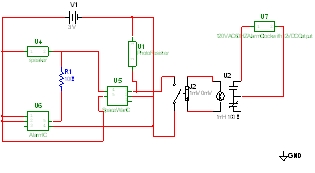
Digital Electronics Education
The goal of Advanced Digital Electronics courses is to connect basic logic gates (combinational circuits) with technical subjects related to binary counter topologies (both Asynchronous and Synchronous), shift registers, memory, and Digital Signal Processors (DSP), which are categorized as sequential...

Altera USB-Blaster plug pinout
The Altera USB-Blaster is an effective USB JTAG programmer, with clones available for US$10 or less. It includes a detailed manual that features a pinout diagram for the JTAG device side. However, the diagram lacks orientation details. A polarization lug...