


Bit Grabber
#bit comparator
#digital logic
#character matching
#computer interface
#binary input
#output trigger
#logic gates
#data processing

Description: When the user sets a character (D0 through D7) from a computer that matches the character programmed on S1A through S1H, the output from J2 becomes low. This device can be used as a test aid to check printer cables or as a control circuit for interfacing with a computer.
The described circuit functions as a character matching system, where the input characters (D0 to D7) are compared against predefined characters stored in a set of switches or inputs (S1A to S1H). The output signal from J2 is activated (pulled low) when a match is detected. This functionality can be implemented using a combination of logic gates, microcontrollers, or programmable logic devices, depending on the complexity and requirements of the application.
In a typical implementation, the input characters D0 to D7 can be received from a computer through a parallel interface. Each input bit corresponds to a character, and the system continuously monitors these inputs. The programmed characters on S1A through S1H can be set using dip switches or similar components, allowing for easy configuration.
When the system identifies a match between the input character and one of the programmed characters, it triggers the output at J2. This output can be utilized in various ways, such as indicating a successful match through an LED, sending a signal to another device, or activating a control mechanism.
The device serves dual purposes: it can function as a test aid for verifying printer cable connections by ensuring that the correct signals are being transmitted, and it can also act as a control circuit for interfacing with computers, enabling automated responses based on character recognition.
In designing this circuit, careful attention should be paid to debounce mechanisms for the switches to avoid false triggering, as well as ensuring that the output signal is compatible with the devices it will interface with. Proper power supply considerations and signal integrity measures should also be implemented to ensure reliable operation in various environments. When the user set character (D0 through D7) from a computer matches the character programmed on S1A through S1H, the output fro m J2 becomes low. This device can be used as a test aid to check printer cable or as a control circuit for interfacing with a computer.
The described circuit functions as a character matching system, where the input characters (D0 to D7) are compared against predefined characters stored in a set of switches or inputs (S1A to S1H). The output signal from J2 is activated (pulled low) when a match is detected. This functionality can be implemented using a combination of logic gates, microcontrollers, or programmable logic devices, depending on the complexity and requirements of the application.
In a typical implementation, the input characters D0 to D7 can be received from a computer through a parallel interface. Each input bit corresponds to a character, and the system continuously monitors these inputs. The programmed characters on S1A through S1H can be set using dip switches or similar components, allowing for easy configuration.
When the system identifies a match between the input character and one of the programmed characters, it triggers the output at J2. This output can be utilized in various ways, such as indicating a successful match through an LED, sending a signal to another device, or activating a control mechanism.
The device serves dual purposes: it can function as a test aid for verifying printer cable connections by ensuring that the correct signals are being transmitted, and it can also act as a control circuit for interfacing with computers, enabling automated responses based on character recognition.
In designing this circuit, careful attention should be paid to debounce mechanisms for the switches to avoid false triggering, as well as ensuring that the output signal is compatible with the devices it will interface with. Proper power supply considerations and signal integrity measures should also be implemented to ensure reliable operation in various environments. When the user set character (D0 through D7) from a computer matches the character programmed on S1A through S1H, the output fro m J2 becomes low. This device can be used as a test aid to check printer cable or as a control circuit for interfacing with a computer.

Help with designing a circuit with logic gates
There are integrated circuits that contain AND, OR, and NOT gates. The inquiry revolves around the existence of a single chip that encompasses all the required logic gates. If such a chip does not exist, specific alternatives should be considered....
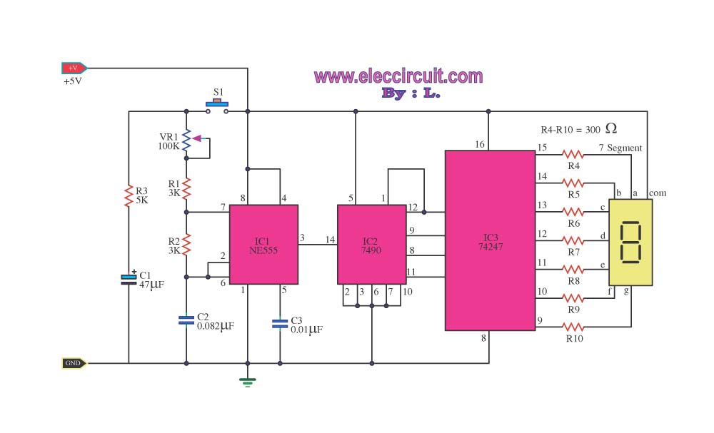
Digital Dice circuit
This digital dice circuit is designed to display numbers effectively. When the spin switch is turned off, it converts the input into a binary format using a diode matrix composed of diodes D1 to D9 (1N4148 or 1N914). This binary...
Digital Electronics Education
The goal of Advanced Digital Electronics courses is to connect basic logic gates (combinational circuits) with technical subjects related to binary counter topologies (both Asynchronous and Synchronous), shift registers, memory, and Digital Signal Processors (DSP), which are categorized as sequential...
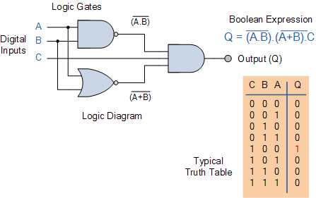
Combinational Logic Circuits using Logic Gates
Electronics tutorial on combinational logic circuits that utilize logic gates to create multiplexers, encoders, and solid-state switches.
Combinational logic circuits are fundamental components in digital electronics, characterized by their ability to produce outputs based solely on the current inputs, without any...

electrical engineering logic gates
Design a circuit with four single-bit inputs X, Y, T, and Z, and a single-bit output E. A two-bit control code word S0S1 determines which of the four inputs is sent to the output (the selection code is not unique)....

Logic Circuits Vs Transistor Power Circuits
Invert a signal to drive FETs with rapid rise and fall times. It was suggested to use an inverter (not a chip) instead of logic chips, which are designed to be either fully ON or OFF. The individual has prior...
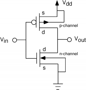
When abstract logic circuits get translated to the electrical equivilant how are conversions from 0 to 1 handled
The fundamental issue presented is the perception that logic gates in a circuit seem to generate power from nothing, which contradicts the principles of physics. For instance, consider two NOT gates connected in series. It appears that the first NOT...
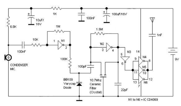
Logic Gates FM Transmitter Circuit
Logic Gates FM Transmitter Circuit Electronic Circuit Schematic Wiring Diagram.
The FM transmitter circuit utilizing logic gates is a fundamental electronic design that operates by modulating a carrier frequency with an audio signal. This circuit typically consists of various logic gates...