


Bus masters diagram
#bus architecture
#AHB-Lite
#FPGA
#ARM CPU
#bus masters
#Logic Tile
#Z bus
#bridge
#system design
#protocol

Description: It is possible to add bus masters to the system, but a different bus architecture would be required since the Integrator/CP uses the AHB-Lite bus protocol, which allows only one bus master (the ARM CPU core). One way to add bus masters in a Logic Tile would be to instantiate a bridge in the IM-LT3 FPGA and split the Z[127:0] bus at the IM-LT3. The custom masters (and slaves) could then exist on the upper segment of this bus, while the Integrator/CP's AHB-Lite System bus would continue to exist on the lower segment of the bus.
The proposed system enhancement involves modifying the existing AHB-Lite bus architecture to accommodate multiple bus masters. The AHB-Lite protocol is inherently designed for single master operation, which limits its flexibility in multi-master configurations. To implement additional bus masters, a bridging mechanism within the IM-LT3 FPGA is suggested. This entails the division of the Z[127:0] bus into two segments: an upper segment dedicated to custom bus masters and slaves, and a lower segment reserved for the existing AHB-Lite System bus controlled by the ARM CPU core.
The implementation of this architecture requires careful consideration of signal integrity and timing, as the introduction of additional masters may lead to increased contention for bus resources. The bridge in the IM-LT3 FPGA will facilitate communication between the two bus segments, ensuring that data can be routed effectively without conflicts. It is essential to design the bridge with appropriate arbitration logic to manage access to the bus and prevent data collisions.
Additionally, the custom bus masters will need to be compatible with the existing bus protocol to ensure seamless integration. This may involve implementing specific interfaces or protocols that allow these masters to communicate effectively with the AHB-Lite System bus.
In conclusion, while the integration of multiple bus masters within the AHB-Lite architecture poses challenges, the proposed solution of utilizing a bridge within the IM-LT3 FPGA offers a viable pathway to enhance system capabilities. This configuration not only expands the functionality of the Logic Tile but also maintains the integrity and performance of the existing AHB-Lite protocol.It is possible to add bus masters to the system, but a different bus architecture would be required, since the Integrator/CP uses the AHB-Lite bus protocol, which allows only one bus master (the ARM CPU core). One way to add bus masters in a Logic Tile would be to instantiate a bridge in the IM-LT3 FPGA, and splitting the Z[127:0] bus at the IM-LT3.
The custom masters (and slaves) could then exist on the upper segment of this bus, and the Integrator/CP's AHB-Lite System bus would continue to exist on the lower segment of the bus.
The proposed system enhancement involves modifying the existing AHB-Lite bus architecture to accommodate multiple bus masters. The AHB-Lite protocol is inherently designed for single master operation, which limits its flexibility in multi-master configurations. To implement additional bus masters, a bridging mechanism within the IM-LT3 FPGA is suggested. This entails the division of the Z[127:0] bus into two segments: an upper segment dedicated to custom bus masters and slaves, and a lower segment reserved for the existing AHB-Lite System bus controlled by the ARM CPU core.
The implementation of this architecture requires careful consideration of signal integrity and timing, as the introduction of additional masters may lead to increased contention for bus resources. The bridge in the IM-LT3 FPGA will facilitate communication between the two bus segments, ensuring that data can be routed effectively without conflicts. It is essential to design the bridge with appropriate arbitration logic to manage access to the bus and prevent data collisions.
Additionally, the custom bus masters will need to be compatible with the existing bus protocol to ensure seamless integration. This may involve implementing specific interfaces or protocols that allow these masters to communicate effectively with the AHB-Lite System bus.
In conclusion, while the integration of multiple bus masters within the AHB-Lite architecture poses challenges, the proposed solution of utilizing a bridge within the IM-LT3 FPGA offers a viable pathway to enhance system capabilities. This configuration not only expands the functionality of the Logic Tile but also maintains the integrity and performance of the existing AHB-Lite protocol.It is possible to add bus masters to the system, but a different bus architecture would be required, since the Integrator/CP uses the AHB-Lite bus protocol, which allows only one bus master (the ARM CPU core). One way to add bus masters in a Logic Tile would be to instantiate a bridge in the IM-LT3 FPGA, and splitting the Z[127:0] bus at the IM-LT3.
The custom masters (and slaves) could then exist on the upper segment of this bus, and the Integrator/CP's AHB-Lite System bus would continue to exist on the lower segment of the bus.

relay interfacing with spartan 3an fpga
The Spartan-3an board features external 5V relay interfacing, as illustrated in the accompanying figure. The ULN2803 acts as a driver for the FPGA I/O lines, with the driver's outputs connected to the relay modules. A PTB connector is available for...
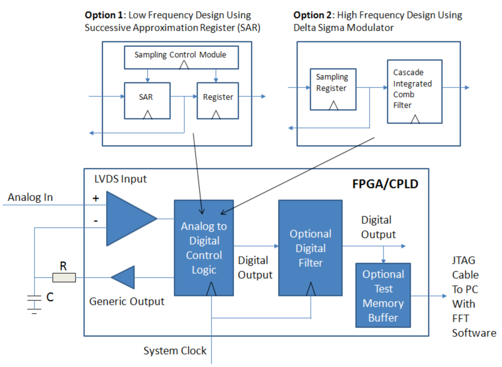
Leveraging FPGA and CPLD digital logic to implement analog to digital converters
Designers of digital systems are familiar with implementing the remnants of their digital design by using FPGAs and CPLDs to connect various processors, memories, and standard function components on their printed circuit board. In addition to these digital functions, FPGAs...
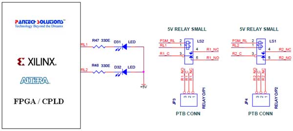
relay interfacing with fpga universal development board
The Universal Development Board features external 5V relay interfacing, as illustrated in the accompanying figure. The ULN2803 is utilized as a driver for FPGA I/O lines, with the driver outputs connected to the relay modules. A PTB connector is provided...
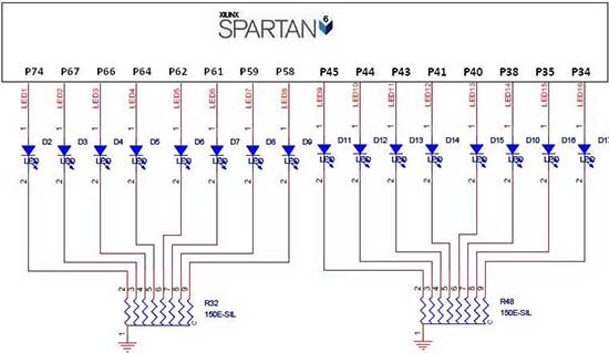
interfacing leds with spartan 6 fpga
The Spartan-6 board features 16 LEDs connected to FPGA I/O pins, as detailed in the table below. The cathode of each LED is connected to ground through a 330-ohm resistor. To illuminate a specific LED, the corresponding FPGA control signal...

FPGA RS232 Serial Interface Circuit
The schematic for this project is a modified version of the CPLD development board schematic. Several new components have been added for this project, and the completed schematic can be viewed below. The main components in the schematic are the...

How to design 65nm FPGA DDR2 memory
This article discusses practical techniques for incorporating "correctness by design" in DDR2 interfaces from a Signal Integrity (SI) perspective, utilizing the current generation of available design tools. It analyzes common DDR2 design errors and the trade-offs between various popular design...
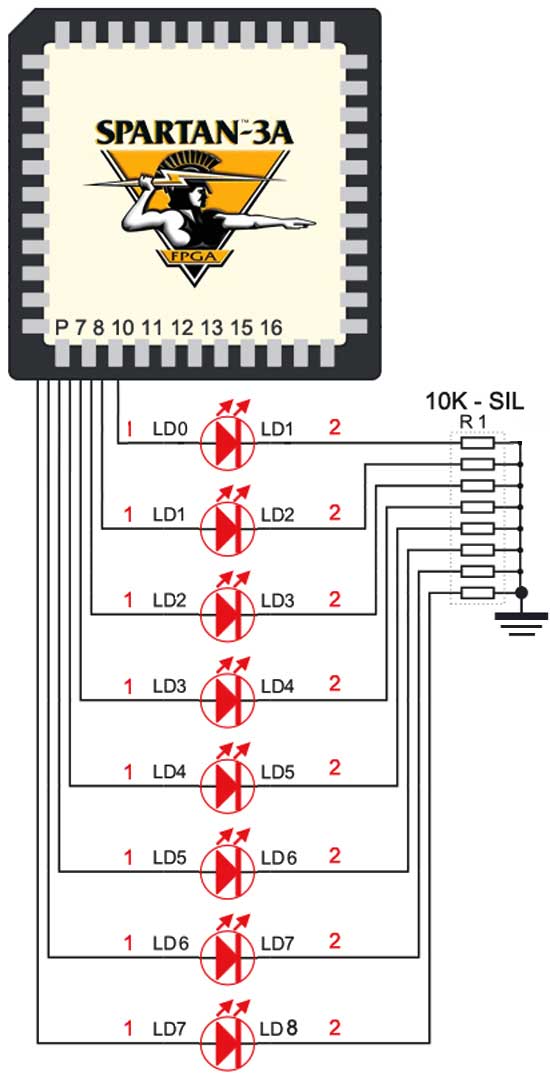
how to interface led with spartan 3an
The Spartan-3an board features eight LEDs connected to FPGA I/O pins. The cathode of each LED is connected to ground through a 330-ohm resistor. To illuminate a specific LED, the corresponding FPGA control signal must be set to High.
The Spartan-3an...

FPGA-based fingerprint identification system schematic
The ASIC design focuses on a highly integrated, low-power solution with a short development cycle to complete an FPGA design aimed at achieving a robust background system, which holds significant practical relevance and broad market potential. The project utilizes the...

LEDs and Switches
The DE2 board features four pushbutton switches, each of which is debounced using a Schmitt Trigger circuit, as shown in Figure 1. The outputs, labeled KEY0 to KEY3, from the Schmitt Trigger are directly connected to the Cyclone II FPGA....