


CD4013 circuit
#CD4013
#D flip-flop
#rising edge
#logic circuit
#CMOS
#sequential logic
#flip-flop
#digital electronics
#clocked logic
#binary storage

Description: The CD4013 is a dual D flip-flop that operates on the rising edge of the clock signal. Its internal block diagram and pin configuration are provided. This device is part of the standard model C043 and the GB model CC4013. Additionally, it has substitutable or interchangeable models such as TC4013, MC14013, C073, SG822, and others.
The CD4013 dual D flip-flop is a versatile digital memory circuit used for storing binary information. Each flip-flop has two inputs, D (data) and CLK (clock), and two outputs, Q and Q' (complement of Q). The flip-flop captures the value present at the D input on the rising edge of the CLK signal, transferring this value to the Q output. The Q' output always reflects the inverse of the Q output.
The internal structure of the CD4013 consists of multiple stages of logic gates configured to form the flip-flop functionality. The device operates with a supply voltage range of 3V to 15V, making it suitable for various applications in both low and high voltage environments. The propagation delay between the clock input and the output state change is typically around 50 nanoseconds at a supply voltage of 5V, which makes it suitable for moderate-speed applications.
Pin configuration is critical for proper integration into circuits. The CD4013 has 14 pins, with the primary pins being:
- Pins 1 and 2: D input and CLK input for the first flip-flop.
- Pins 3 and 4: Q output and Q' output for the first flip-flop.
- Pins 5 and 6: D input and CLK input for the second flip-flop.
- Pins 7 and 8: Q output and Q' output for the second flip-flop.
- Pins 11, 12, 13, and 14 are used for power supply and ground connections.
The CD4013 is widely used in digital circuits for applications such as data storage, state machines, and frequency division. Its ability to interface with various logic families enhances its applicability in diverse electronic designs. The interchangeable models (TC4013, MC14013, etc.) offer flexibility in sourcing components while maintaining compatibility with the original design specifications.CD4013 dual D flip-flop on the rising edge. Its internal block diagram and pins are shown. Ministry of standard model C043, GB model CC4013, substitutable or interchangeable models TC4013, MC14013, C073, SG822 and the like.
The CD4013 dual D flip-flop is a versatile digital memory circuit used for storing binary information. Each flip-flop has two inputs, D (data) and CLK (clock), and two outputs, Q and Q' (complement of Q). The flip-flop captures the value present at the D input on the rising edge of the CLK signal, transferring this value to the Q output. The Q' output always reflects the inverse of the Q output.
The internal structure of the CD4013 consists of multiple stages of logic gates configured to form the flip-flop functionality. The device operates with a supply voltage range of 3V to 15V, making it suitable for various applications in both low and high voltage environments. The propagation delay between the clock input and the output state change is typically around 50 nanoseconds at a supply voltage of 5V, which makes it suitable for moderate-speed applications.
Pin configuration is critical for proper integration into circuits. The CD4013 has 14 pins, with the primary pins being:
- Pins 1 and 2: D input and CLK input for the first flip-flop.
- Pins 3 and 4: Q output and Q' output for the first flip-flop.
- Pins 5 and 6: D input and CLK input for the second flip-flop.
- Pins 7 and 8: Q output and Q' output for the second flip-flop.
- Pins 11, 12, 13, and 14 are used for power supply and ground connections.
The CD4013 is widely used in digital circuits for applications such as data storage, state machines, and frequency division. Its ability to interface with various logic families enhances its applicability in diverse electronic designs. The interchangeable models (TC4013, MC14013, etc.) offer flexibility in sourcing components while maintaining compatibility with the original design specifications.CD4013 dual D flip-flop on the rising edge. Its internal block diagram and pins are shown. Ministry of standard model C043, GB model CC4013, substitutable or interchangeable models TC4013, MC14013, C073, SG822 and the like.

Optical-cmos-coupler
Standard CMOS logic operates with supply voltages as low as 3 V and is specified for a maximum current sinking/sourcing capability of 30 pA. To drive the infrared emitting diode (IRED) when utilizing CMOS to control an optocoupler, it is...
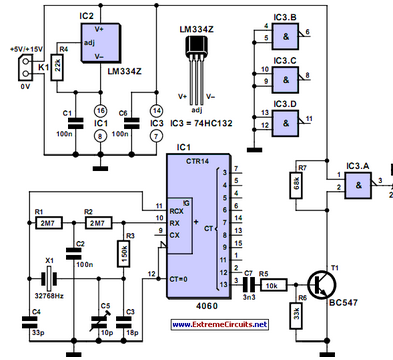
Thrifty 2Hz Clock
CMOS circuits are recognized for their low current consumption, which is especially significant for battery-powered applications. However, oscillators frequently face challenges related to...
CMOS (Complementary Metal-Oxide-Semiconductor) technology is widely utilized in the design of integrated circuits due to its advantageous characteristics,...

Removing pop from a CMOS switch
A simple audio switching circuit is experiencing issues. The circuit utilizes a CD40106 Schmitt Trigger in conjunction with a CD4066 CMOS switch to route audio signals.
The circuit design incorporates a CD40106 Schmitt Trigger, which is essential for providing clean signal...

Flip-Flop Debouncer Switch
This circuit utilizes a 74HC74 flip-flop, although any CMOS variant of this component can be employed. IC1A functions as a true/complement buffer. Resistors R1 and R2 ensure that IC1A exits the reset state prior to the clock edge occurrence. Resistor...
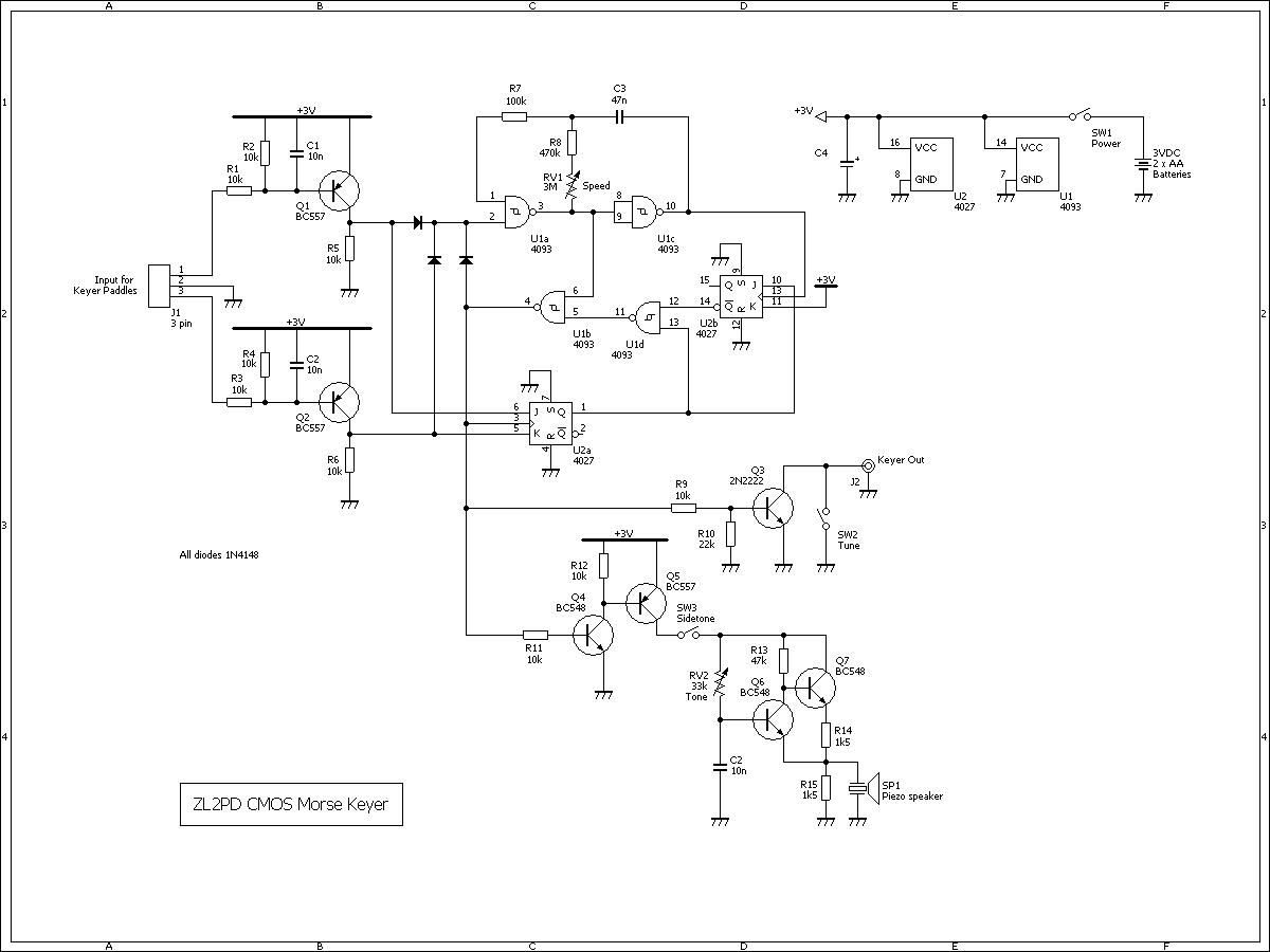
Morse Keyer Redesign and Rebuild
Two inexpensive CMOS integrated circuits and a few transistors were sufficient to convert an old TTL automatic Morse keyer into a low-current, lightweight, battery-powered iambic Morse keyer. Over the last couple of years, the aging Accu-Keyer ceased functioning. This device...

Hydro alarm circuit diagram using CMOS
The circuit diagram is straightforward and operates as follows: the N1 Schmitt trigger functions as an oscillator, producing a frequency of approximately 1 kHz. When there is sufficient water in the tank, alternating voltage flows from electrode A to electrode...

Cmos line receiver
The trip point is set halfway between the supplies by R1 and R2; R3 provides over 200 mV of hysteresis to increase noise immunity. The maximum frequency of operation is about 300 kHz. If response to TTL levels is desired,...

Two Interlocked Toggle Switches - Cmos 4013
This versatile circuit offers a selection of different switching modes. It can function as two entirely separate toggle switches, with each push button successively energizing and de-energizing its corresponding relay. Alternatively, the two switches can be interconnected with diodes to...

Cmos Based Vehicle Anti-Theft Alarm
This circuit features automatic exit and entry delays, an optional instant alarm zone, an optional intermittent siren output, and an automatic reset. By adding external relays, the vehicle can be immobilized and the lights can be flashed. The alarm is...