


Frequency doubler II
#frequency doubler
#CMOS
#NAND gate
#4011
#digital circuit
#pulse generator
#logic gates
#differentiating network

Description: This frequency doubler uses one CMOS quad, two input NAND gate package type 4011. The frequency doubler proper consists of an inverter IC1B, two differentiating networks R1/C1, R2/C2 and NAND gate IC1A, IC1C and IC1D function as input and output buffers. In Fig.2 exist the pulses in different points of circuit.
The described frequency doubler circuit utilizes a CMOS quad two-input NAND gate IC, specifically the 4011 package, to achieve frequency multiplication. The core operation relies on the conversion of an input frequency to its double by employing a combination of logic gates and differentiating networks.
The circuit is structured around an inverter (IC1B) that is responsible for inverting the input signal. This inversion is crucial as it helps to create the necessary phase shifts required for the frequency doubling process. The differentiating networks, composed of resistors (R1, R2) and capacitors (C1, C2), play a significant role in shaping the input waveform. These networks convert the square wave input into a series of sharp pulses, which are essential for effective triggering of the NAND gates.
The NAND gates (IC1A, IC1C, and IC1D) serve multiple functions in this circuit. IC1A acts as the primary logic gate to process the differentiated signals, while IC1C and IC1D are utilized as buffers to ensure that the output signals maintain their integrity and drive capabilities. This arrangement allows for a robust output that can effectively double the frequency of the input signal.
The output of the circuit presents a waveform that oscillates at twice the frequency of the original input, demonstrating the effectiveness of the frequency doubler. The arrangement of components ensures minimal signal degradation, allowing for a clean and precise output waveform. The use of CMOS technology contributes to low power consumption and high-speed operation, making this frequency doubler suitable for various applications in signal processing and communication systems.
In summary, the frequency doubler circuit based on the CMOS quad NAND gate 4011 is a well-structured design that efficiently converts an input frequency into its double using inverting and buffering techniques, along with differentiating networks for optimal signal shaping. This frequency doubler uses one CMOS quad, two input NAND gate package type 4011. The frequency doubler proper consists of an inverter IC1B, two differentiating networks R1/C1, R2/C2 and NAND gate IC1A, IC1C and IC1D function as input and output buffers. In Fig.2 exist the pulses in different points of circuit.
The described frequency doubler circuit utilizes a CMOS quad two-input NAND gate IC, specifically the 4011 package, to achieve frequency multiplication. The core operation relies on the conversion of an input frequency to its double by employing a combination of logic gates and differentiating networks.
The circuit is structured around an inverter (IC1B) that is responsible for inverting the input signal. This inversion is crucial as it helps to create the necessary phase shifts required for the frequency doubling process. The differentiating networks, composed of resistors (R1, R2) and capacitors (C1, C2), play a significant role in shaping the input waveform. These networks convert the square wave input into a series of sharp pulses, which are essential for effective triggering of the NAND gates.
The NAND gates (IC1A, IC1C, and IC1D) serve multiple functions in this circuit. IC1A acts as the primary logic gate to process the differentiated signals, while IC1C and IC1D are utilized as buffers to ensure that the output signals maintain their integrity and drive capabilities. This arrangement allows for a robust output that can effectively double the frequency of the input signal.
The output of the circuit presents a waveform that oscillates at twice the frequency of the original input, demonstrating the effectiveness of the frequency doubler. The arrangement of components ensures minimal signal degradation, allowing for a clean and precise output waveform. The use of CMOS technology contributes to low power consumption and high-speed operation, making this frequency doubler suitable for various applications in signal processing and communication systems.
In summary, the frequency doubler circuit based on the CMOS quad NAND gate 4011 is a well-structured design that efficiently converts an input frequency into its double using inverting and buffering techniques, along with differentiating networks for optimal signal shaping. This frequency doubler uses one CMOS quad, two input NAND gate package type 4011. The frequency doubler proper consists of an inverter IC1B, two differentiating networks R1/C1, R2/C2 and NAND gate IC1A, IC1C and IC1D function as input and output buffers. In Fig.2 exist the pulses in different points of circuit.

Logic Circuits Vs Transistor Power Circuits
Invert a signal to drive FETs with rapid rise and fall times. It was suggested to use an inverter (not a chip) instead of logic chips, which are designed to be either fully ON or OFF. The individual has prior...

HORN CIRCUIT_FOR_MOTORCYCLE_USE
Gates U1-a and U1-b of the 4093 quad 2-input NAND Schmitt trigger are connected in variable, low-frequency square-wave oscillator circuits. The output of gate U1-a is connected to one of the inputs of gate U1-b. The square-wave output of gate...

design cdba 018 m cmos
The design of a current difference buffer amplifier (CDBA) circuit for fabrication in a commercial CMOS semiconductor process allows for the versatile application of this component across various uses.
The current difference buffer amplifier (CDBA) is a specialized analog circuit that...

Pulse DemodulatorCircuit
The Pulse Demodulator, as illustrated in the accompanying image, consists of a CMOS Hex Inverter. This circuit is capable of performing envelope detection on amplitude pulses.
The Pulse Demodulator utilizing a CMOS Hex Inverter is designed to extract the envelope of...

Audio Signal Generator
A couple of inexpensive CMOS integrated circuits are utilized to digitally generate audio sine waves across a broad frequency range in this compact battery-operated test instrument. The oscillator features both unbalanced and balanced outputs. Signal generators are frequently used in...

LONG PERIOD TIMER
This circuit utilizes the 7240 CMOS programmable timer chip (IC3), which has an accuracy of 0.5 percent. It features a time-base generator, with the frequency determined by a resistor and a capacitor. The basic time period is RC seconds; with...

Lantern controller circuit diagram of a two-dimensional
The circuit primarily consists of the NAND gate IC1 (CD4096), a counting/timing distribution circuit IC2 (CD4017), an analog electronic switch IC3 (CD4066), and a D flip-flop IC4 (CD40174), along with other components. The controller is capable of managing the progressive...

Repeating Interval Timer 2
This is a simpler repeating timer circuit. It uses just one CMOS IC wired as an asymmetric oscillator. The length of time the relay remains energized and the length of time it remains de-energized are set independently.
The repeating timer circuit...
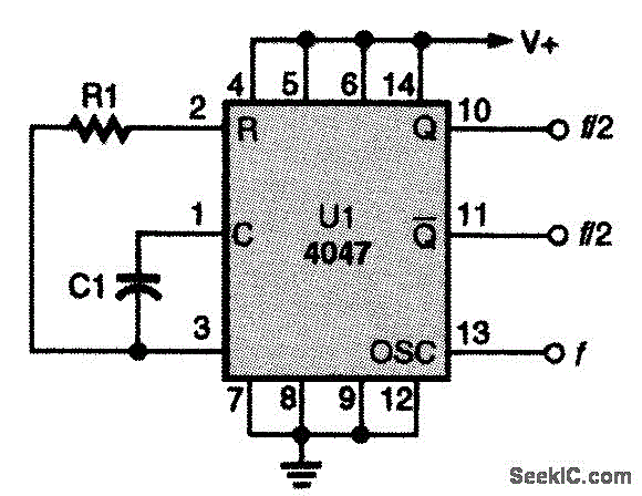
CD4047 CMOS OSCILLATOR
This CMOS square-wave oscillator utilizes the 4047 multivibrator circuit, suitable for both monostable (one-shot) and astable applications. In the provided configuration, the 4047 operates as an astable multivibrator. The circuit features three outputs from the 4047, with the first being...