


integrated circuit Wiring a 74LS259 (addressable latch)
#74LS259
#addressable latch
#digital logic
#TTL
#latch circuit
#logic IC
#binary data
#circuit wiring
#hardware testing
#no microcontroller

Description: The objective is to utilize a 74LS259 8-bit addressable latch without the involvement of a microcontroller, in order to fully comprehend the wiring and functionality.
The 74LS259 is an 8-bit addressable latch that is commonly used in digital circuits for storing binary data. It features eight data inputs (D0 to D7), an address input (A0 to A2), a latch enable input (LE), and an output enable input (OE). The device operates on a positive logic level and is typically powered by a +5V supply.
To configure the 74LS259, the first step involves connecting the power supply. The Vcc pin should be connected to +5V, while the ground (GND) pin should be connected to the system ground. The data inputs (D0 to D7) can be connected to various digital signal sources, such as switches or other logic devices, which will provide the binary data to be latched.
The address inputs (A0 to A2) are used to select which of the eight data inputs will be latched. These inputs should be connected to a binary counter or manually set to select the desired input. The latch enable (LE) input must be driven high to allow data to be latched. When LE is low, the output will retain the last latched value.
The output enable (OE) input, when driven low, allows the latched data to be output on the Q0 to Q7 pins. If OE is high, the outputs will be in a high-impedance state, effectively disconnecting them from the circuit. This feature is useful for multiplexing applications where multiple devices share the same output lines.
For testing purposes, a simple circuit can be set up with push buttons connected to the data inputs and a binary counter connected to the address lines. By pressing the buttons, different binary values can be latched, and the corresponding output can be monitored. This approach allows for a comprehensive understanding of the latch's operation without requiring a microcontroller, providing a clear insight into the device's functionality and behavior in a digital circuit.I`m trying to use a 74LS259 8 bit addressable latch. I`m trying to get it working without a micro-controller first to ensure that I understanding the wiring 100%.
The 74LS259 is an 8-bit addressable latch that is commonly used in digital circuits for storing binary data. It features eight data inputs (D0 to D7), an address input (A0 to A2), a latch enable input (LE), and an output enable input (OE). The device operates on a positive logic level and is typically powered by a +5V supply.
To configure the 74LS259, the first step involves connecting the power supply. The Vcc pin should be connected to +5V, while the ground (GND) pin should be connected to the system ground. The data inputs (D0 to D7) can be connected to various digital signal sources, such as switches or other logic devices, which will provide the binary data to be latched.
The address inputs (A0 to A2) are used to select which of the eight data inputs will be latched. These inputs should be connected to a binary counter or manually set to select the desired input. The latch enable (LE) input must be driven high to allow data to be latched. When LE is low, the output will retain the last latched value.
The output enable (OE) input, when driven low, allows the latched data to be output on the Q0 to Q7 pins. If OE is high, the outputs will be in a high-impedance state, effectively disconnecting them from the circuit. This feature is useful for multiplexing applications where multiple devices share the same output lines.
For testing purposes, a simple circuit can be set up with push buttons connected to the data inputs and a binary counter connected to the address lines. By pressing the buttons, different binary values can be latched, and the corresponding output can be monitored. This approach allows for a comprehensive understanding of the latch's operation without requiring a microcontroller, providing a clear insight into the device's functionality and behavior in a digital circuit.I`m trying to use a 74LS259 8 bit addressable latch. I`m trying to get it working without a micro-controller first to ensure that I understanding the wiring 100%.

Adjustable TTL clock
The symmetry of the square-wave output is maintained by connecting the right side of resistor R2 through resistor R3 to the output of the third amplifier stage. This configuration alters the charging current to the capacitors in proportion to the...

TTL Load circuit
A device that conducts electric current and converts electrical energy into another form. Power consumed by a device or circuit while performing its function can be represented by a resistor and capacitor. The capacitor in the load circuit represents the...
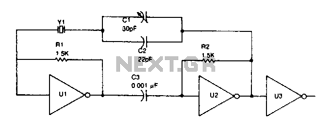
TTL oscillator
TTL inverter stages, U1 and U2, are cross-connected with a crystal Y1. A resistor in each stage biases the normally digital gates into a region where they operate as amplifiers. Inverter stage U3 is used as a buffer.
The circuit consists...

Ttl logic tester
Gates G1 and G2, along with resistors R1 and R2, create a straightforward voltage monitor with a trip point set at 1 volt. Gate G3 functions as an inverter. The display section of the tester features a common anode alphanumeric...

TTL signal levels using a serial port MAX232
A PC’s serial port provides signal lines that you can use to expand the number of input signals. With some additional circuitry tied to these lines, you can use the port to test digital TTL logic-level circuits. You just need...

Ttl-compatible crystal oscillator
Adjust Rl for approximately 2 volts at the output of the first gate. Additionally, adjust Cl for optimal output.
In the context of electronic circuit design, the output voltage of a gate, such as a logic gate or operational amplifier, is...

Power Supply for TTL
In the circuit shown below, if the voltage at the output terminals rises above 6.2V, zener conducts charging capacitor C4. This voltage will fire the silicon-controlled rectifier (SCR), which quickly shorts across the supply rails blowing the fuse. The regulator...

LCD_controller
The clip sync output to TTL level appears to require additional time to accommodate extra components on the board. As a temporary solution, a ZPD4.7 (4.7 V Zener Diode) should be placed between SG and ground at the power switch...

Sine- And Square-Wave Ttl Oscillator
A TTL oscillator utilizing a Quad NAND Gate can operate with fundamental crystals ranging from 1 to 10 MHz. The sine wave output is derived directly from the crystal, which functions as its own filter, producing a relatively clean sine...