


Split Phase-Data Synchronizer and Decoder
#synchronizer
#decoder
#split-phase
#data signal
#binary digits
#timing diagram
#periodic rate
#waveform

Description: Waveform A is a timing diagram that illustrates a split-phase data signal. It consists of a series of binary digits that occur at a periodic rate, with a specified duration for each bit.
The timing diagram of Waveform A provides a visual representation of the split-phase data signaling method, which is commonly used in digital communication systems. In this format, data is transmitted in two distinct phases, allowing for improved synchronization and error detection. The binary digits, or bits, are represented as high and low voltage levels, corresponding to logical '1' and '0', respectively.
Each bit in the waveform has a defined duration, which is crucial for ensuring that the receiving end can accurately interpret the signal. The periodic nature of the signal is characterized by a consistent time interval between the transitions of each bit, which is essential for maintaining the integrity of the data transmission.
In a practical application, the split-phase data signal can be utilized in various communication protocols, such as UART (Universal Asynchronous Receiver-Transmitter) or SPI (Serial Peripheral Interface). The timing diagram aids in understanding the timing relationships between the bits, including rise and fall times, as well as the setup and hold times required for reliable data sampling.
The waveform's characteristics can be further analyzed to determine parameters such as the frequency of the signal, the duty cycle, and potential signal integrity issues that may arise due to noise or distortion. Overall, the timing diagram serves as a fundamental tool for engineers to design, troubleshoot, and optimize digital communication systems.Waveform A is timing diagram that shows A split-phase data signal. It consist of a series of binary digits that occur at a periodic rate. Duration of each bit..
The timing diagram of Waveform A provides a visual representation of the split-phase data signaling method, which is commonly used in digital communication systems. In this format, data is transmitted in two distinct phases, allowing for improved synchronization and error detection. The binary digits, or bits, are represented as high and low voltage levels, corresponding to logical '1' and '0', respectively.
Each bit in the waveform has a defined duration, which is crucial for ensuring that the receiving end can accurately interpret the signal. The periodic nature of the signal is characterized by a consistent time interval between the transitions of each bit, which is essential for maintaining the integrity of the data transmission.
In a practical application, the split-phase data signal can be utilized in various communication protocols, such as UART (Universal Asynchronous Receiver-Transmitter) or SPI (Serial Peripheral Interface). The timing diagram aids in understanding the timing relationships between the bits, including rise and fall times, as well as the setup and hold times required for reliable data sampling.
The waveform's characteristics can be further analyzed to determine parameters such as the frequency of the signal, the duty cycle, and potential signal integrity issues that may arise due to noise or distortion. Overall, the timing diagram serves as a fundamental tool for engineers to design, troubleshoot, and optimize digital communication systems.Waveform A is timing diagram that shows A split-phase data signal. It consist of a series of binary digits that occur at a periodic rate. Duration of each bit..

decoder circuit
The PPI-8255 is a general-purpose I/O programmable interface that is typically connected directly to a computer bus. This article demonstrates that the card can serve dual purposes: as an expander port and for direct I/O functionality. The card can be...

A practical MS Decoder Circuit
The schematic diagram of the MS Decoder may appear complex, but it is relatively straightforward. Initially, both the Mid and Side signals are buffered using unity gain inverting buffers, which are constructed around IC1b and IC2b. This buffering serves two...

decoder
There is a version without SMD, referred to as version 2.1, which is slightly larger (80 x 100 mm) and features dual drivers capable of handling a 1A load. It operates using the same software. The input voltage from the...

4-channel SQ logic decoder
4-channel SQ logic decoder with a current drain of 75 mA at 20 volts. The input impedance is 2M ohms, and the output impedance is 2K ohms (courtesy of GTE Sylvania Incorporated).
The 4-channel SQ logic decoder is an integrated circuit...
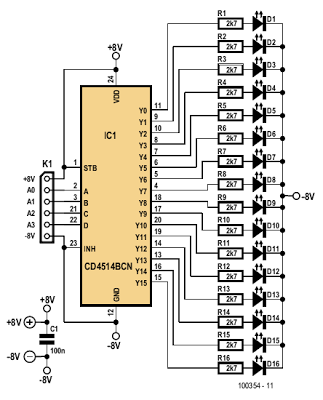
Simple Indicator for Dynamic Limiter Schematic Diagram
The indicator described here is specifically designed for adjusting the dynamic limiter outlined elsewhere in this edition and checking if the maximum level of the reference voltage (P1) requires modification. A 4-to-16 decoder integrated circuit (IC) of type 4514 is...
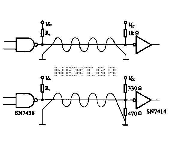
Transmission distance of 5m or less circuit configuration
The circuit configuration for data signal output is designed to optimize transmission distance. It includes an output terminal connected to a pull-up resistor at the receiving end, which works in conjunction with two pull-up and pull-down resistors.
The described circuit configuration...

Background music decoder
This circuit is a background music (SCA) decoder designed to process an input demodulated (multiplex) FM signal. The NE565, a Phase Locked Loop (PLL) integrated circuit, serves as the foundation for this design.
The background music (SCA) decoder circuit utilizes the...

Rectangular/Triangular Waveform Converter
Many function generators utilize a rectangular waveform generator that comprises a Schmitt trigger and an integrator. The triangular signal generated by the integrator is subsequently transformed into a sinusoidal signal using a diode network. The converter described here operates inversely,...

Sca background music decoder
A resistive voltage divider is utilized to establish a bias voltage for the input (pins 2 and 3). The demodulated FM signal is introduced to the input through a two-stage high-pass filter, which serves to provide capacitive coupling and to...