


Switch Debouncer With Auto Repeat
#switch debouncer
#pushbutton
#hysteresis
#pulse generator
#digital circuit
#debouncing
#auto repeat
#logic gate
#signal conditioning

Description: This circuit generates an output pulse when the pushbutton SW1 is pressed. It also functions as a hysteresis gate oscillator. Diode D1 and resistor R2 introduce asymmetry into the circuit. The delay before repeat time (DBRT) is influenced by the start-up conditions of the oscillator: capacitor C1 must charge from zero to the upper gate threshold rather than to the lower threshold. The auto repeat time is determined by the gate hysteresis, which is less than 1 V for the 74HCT14 gate, with DBRT equal to 0.7 times the upper gate threshold hysteresis. The upper gate threshold is 2.3 V for the HCT14, with resistor R1 being much smaller than R3 and R2 being much smaller than R1.
This circuit can be analyzed in terms of its key components and their interactions. The pushbutton switch SW1 acts as the input trigger, initiating the pulse generation when pressed. The hysteresis gate oscillator, utilizing a 74HCT14 Schmitt trigger, provides a stable output by ensuring that the output state changes only when the input crosses specific voltage thresholds.
Diode D1 serves to create asymmetry in the charge and discharge cycles of capacitor C1, which is critical for defining the timing characteristics of the oscillator. The resistor R2 plays a role in controlling the discharge path of C1, thereby influencing the time it takes for the capacitor to reach the upper gate threshold of 2.3 V.
The DBRT is a crucial parameter that defines the delay before the oscillator can repeat its cycle. It is determined by the time required for C1 to charge to the upper threshold, which is a function of the circuit's resistive and capacitive components. The hysteresis effect, characterized by a voltage difference of less than 1 V, ensures that noise does not cause false triggering of the output pulse.
The relationships between the resistors R1, R2, and R3 are significant in ensuring that R1 is much smaller than R3, and R2 is much smaller than R1. This configuration allows for optimal performance of the oscillator, ensuring that the timing and pulse generation are reliable and consistent. The circuit design is thus a balance of component values that achieves the desired output characteristics while maintaining stability and responsiveness in pulse generation. This circuit produces an output pulse when SW1 (pushbutton) is depressed. It also becomes a hysteresis ga te oscillator. Dl and R2 add asymmetry. The DBRT (delay before repeat time) is caused by the oscillator start-up conditions: CI has to change from zero to the upper gate threshold rather than to the lower threshold. The auto repeat time: Gate hysteresis « 1 V for 74HCT14 gate, DBRT= 0.7T (upper gate threshold hysteresis).
Upper gate threshold 2.3 V for HCT14, Ri<
Related Circuits
This circuit can be analyzed in terms of its key components and their interactions. The pushbutton switch SW1 acts as the input trigger, initiating the pulse generation when pressed. The hysteresis gate oscillator, utilizing a 74HCT14 Schmitt trigger, provides a stable output by ensuring that the output state changes only when the input crosses specific voltage thresholds.
Diode D1 serves to create asymmetry in the charge and discharge cycles of capacitor C1, which is critical for defining the timing characteristics of the oscillator. The resistor R2 plays a role in controlling the discharge path of C1, thereby influencing the time it takes for the capacitor to reach the upper gate threshold of 2.3 V.
The DBRT is a crucial parameter that defines the delay before the oscillator can repeat its cycle. It is determined by the time required for C1 to charge to the upper threshold, which is a function of the circuit's resistive and capacitive components. The hysteresis effect, characterized by a voltage difference of less than 1 V, ensures that noise does not cause false triggering of the output pulse.
The relationships between the resistors R1, R2, and R3 are significant in ensuring that R1 is much smaller than R3, and R2 is much smaller than R1. This configuration allows for optimal performance of the oscillator, ensuring that the timing and pulse generation are reliable and consistent. The circuit design is thus a balance of component values that achieves the desired output characteristics while maintaining stability and responsiveness in pulse generation. This circuit produces an output pulse when SW1 (pushbutton) is depressed. It also becomes a hysteresis ga te oscillator. Dl and R2 add asymmetry. The DBRT (delay before repeat time) is caused by the oscillator start-up conditions: CI has to change from zero to the upper gate threshold rather than to the lower threshold. The auto repeat time: Gate hysteresis « 1 V for 74HCT14 gate, DBRT= 0.7T (upper gate threshold hysteresis).
Upper gate threshold 2.3 V for HCT14, Ri<
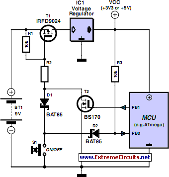
The Gentle Touch
Modern consumer appliances often lack a traditional mains switch. Instead, they are activated and deactivated via a button on a remote control, similar to other functions. This circuit illustrates how a device can be toggled on and off using a...

Pulse Generator And Signal TracerCircuit
This simple circuit generates narrow pulses at a frequency of approximately 700-800 Hz. The pulses, which contain harmonics extending into the MHz range, can be injected into audio or radio-frequency stages of amplifiers and receivers for testing purposes. A high-pitched...
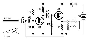
Pulse-Generator & Signal-Tracer
This simple circuit generates narrow pulses at about 700-800Hz frequency. The pulses, containing harmonics up to the MHz region, can be injected into audio or radio-frequency stages of amplifiers, receivers and the like for testing purposes. A high-pitched tone can...

PULSE DELAY
When a GATE signal (between 3V and 15V) is applied, the capacitor C5 functions as a differentiator, converting the gate signal into a brief positive pulse with a width of 10 ms. Diode D1 protects the circuit from negative voltages....
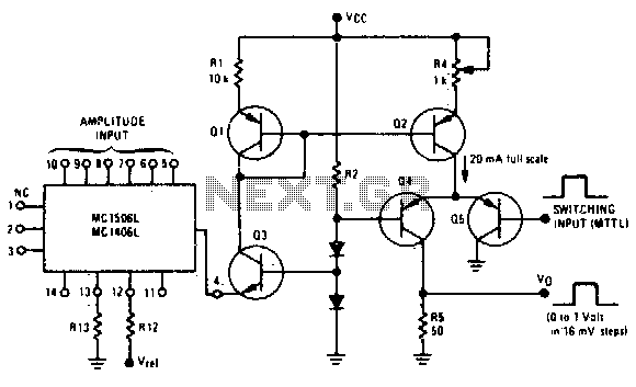
Programmable pulse generator
Fast rise and fall times necessitate the utilization of high-speed switching transistors for the differential pair, Q4 and Q5. Linear ramps and sine waves can be produced using the suitable reference input.
The circuit employs high-speed switching transistors, specifically Q4 and...

Pulse Signal Generator
The volt-ampere characteristics of a tunnel diode exhibit an S-shaped curve. The peak current point, referred to as point P, represents the maximum current, while the valley point, denoted as point V, indicates the minimum current. Key parameters of the...
Pulse Signal Generator
The volt-ampere characteristics of a tunnel diode exhibit an S-shaped curve. The peak current point, referred to as point P, represents the maximum current, while the valley point, denoted as point V, indicates the minimum current. Key parameters of the...

About Area 50
This circuit divides a 10 MHz reference signal to produce outputs of 1, 10, 100, or 1000 pulses per second. The pulse width can be selected using jumpers, offering multiple options. A synchronization input aligns the output pulses with an...

Signal Conditioning Analog Front-end for Microcontrollers
The I/O board incorporates 16-bit resolution voltage analog inputs and outputs, along with a 4-20mA current loop transmitter and receiver for microcontroller applications. The document discusses amplifier circuits and schematics, including a signal conditioning variable gain amplifier, analog filter, and...