


Negative oxygen ion generator 4
#negative oxygen ion
#rectifier
#pulse oscillation
#high voltage
#transistor
#capacitor
#diode
#voltage generation

Description: This negative oxygen ion generator circuit consists of a full-wave dual voltage rectifier circuit, a pulse oscillation circuit, and a negative high voltage generation circuit, as illustrated in figure 9-116. The dual voltage rectifier circuit is constructed using diodes VD1 and VD2, along with capacitors C1 and C2. The pulse oscillation circuit includes a transistor (V), resistor R1, a potentiometer (RP), capacitor C3, diode VD3, and one winding of the boost transformer (T). The negative high voltage generation circuit comprises two windings of T, a high voltage silicon rectifier stack (VD4), resistor R2, and capacitor C4.
The negative oxygen ion generator circuit is designed to produce a flow of negative oxygen ions, which can be beneficial for air purification and improving air quality. The full-wave dual voltage rectifier circuit converts the incoming AC voltage into a pulsating DC voltage, utilizing diodes VD1 and VD2 for rectification. Capacitors C1 and C2 serve to smooth the output voltage, ensuring a more stable DC supply for the subsequent stages of the circuit.
The pulse oscillation circuit is crucial for generating the necessary high-frequency oscillations that drive the negative ion generation process. Transistor V acts as a switch, controlled by the voltage across potentiometer RP, which allows for fine-tuning the oscillation frequency. Resistor R1 provides necessary biasing for the transistor, while capacitor C3 aids in determining the oscillation frequency along with the characteristics of diode VD3, which rectifies the oscillating signal to maintain the pulse shape required for the boost transformer.
The boost transformer (T) plays a vital role in stepping up the voltage to the high levels required for ion generation. The negative high voltage generation circuit utilizes two windings of the transformer to achieve the desired output voltage. The high voltage silicon rectifier stack (VD4) is employed to convert the high-frequency AC output from the transformer into a high DC voltage suitable for ion generation. Resistor R2 and capacitor C4 are included to filter and stabilize the high voltage output, ensuring that the circuit operates efficiently and reliably.
Overall, this circuit design integrates various components to effectively generate negative oxygen ions, contributing to applications in air purification and enhancing environmental conditions. The careful selection and arrangement of components are essential for optimizing performance and ensuring the longevity of the device.This negative oxygen ion generator circuit is composed of full wave dual voltage rectifier circuit, pulse oscillation circuit and negative high voltage generation circuit, it is shown in the figure 9-116. The dual voltage rectifier circuit is made of diodes VD1, VD2, and capacitors C1, C2. The pulse oscillation circuit consists of transistor V, re sistor R1, potentiometer RP, capacitor C3, diode VD3 and once winding of boost transformer T. The negative high voltage generation circuit is composed of twice winding of T, high voltage silicon rectifier stack VD4, resistor R2 and capacitor C4.
The negative oxygen ion generator circuit is designed to produce a flow of negative oxygen ions, which can be beneficial for air purification and improving air quality. The full-wave dual voltage rectifier circuit converts the incoming AC voltage into a pulsating DC voltage, utilizing diodes VD1 and VD2 for rectification. Capacitors C1 and C2 serve to smooth the output voltage, ensuring a more stable DC supply for the subsequent stages of the circuit.
The pulse oscillation circuit is crucial for generating the necessary high-frequency oscillations that drive the negative ion generation process. Transistor V acts as a switch, controlled by the voltage across potentiometer RP, which allows for fine-tuning the oscillation frequency. Resistor R1 provides necessary biasing for the transistor, while capacitor C3 aids in determining the oscillation frequency along with the characteristics of diode VD3, which rectifies the oscillating signal to maintain the pulse shape required for the boost transformer.
The boost transformer (T) plays a vital role in stepping up the voltage to the high levels required for ion generation. The negative high voltage generation circuit utilizes two windings of the transformer to achieve the desired output voltage. The high voltage silicon rectifier stack (VD4) is employed to convert the high-frequency AC output from the transformer into a high DC voltage suitable for ion generation. Resistor R2 and capacitor C4 are included to filter and stabilize the high voltage output, ensuring that the circuit operates efficiently and reliably.
Overall, this circuit design integrates various components to effectively generate negative oxygen ions, contributing to applications in air purification and enhancing environmental conditions. The careful selection and arrangement of components are essential for optimizing performance and ensuring the longevity of the device.This negative oxygen ion generator circuit is composed of full wave dual voltage rectifier circuit, pulse oscillation circuit and negative high voltage generation circuit, it is shown in the figure 9-116. The dual voltage rectifier circuit is made of diodes VD1, VD2, and capacitors C1, C2. The pulse oscillation circuit consists of transistor V, re sistor R1, potentiometer RP, capacitor C3, diode VD3 and once winding of boost transformer T. The negative high voltage generation circuit is composed of twice winding of T, high voltage silicon rectifier stack VD4, resistor R2 and capacitor C4.

Transistor Tester
This circuit can measure both small signal hfe and DC current gain hFE of a low to medium power transistor.
The circuit is designed to evaluate the current gain characteristics of low to medium power transistors by measuring both the small...

100w inverter circuit
This is a 100-watt transistor inverter circuit diagram that features a straightforward design. The circuit utilizes only transistors, eliminating the need for integrated circuits. It converts a 12V battery input into a 220V output with a 50Hz square wave signal....
metal detector circuit
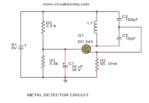
This circuit diagram represents a low-cost metal detector utilizing a single transistor circuit in conjunction with an old pocket radio. It operates as a Colpitts oscillator functioning within the medium band frequency range, with the radio tuned to the same...
expandable transistor based burglar alarm
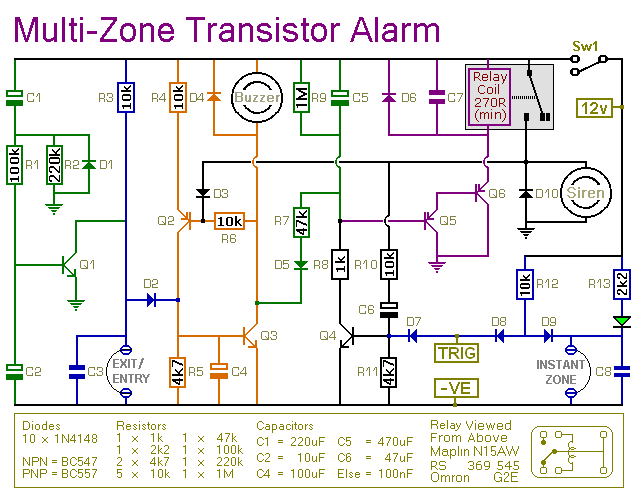
This transistor-based alarm system incorporates automatic exit and entry delays, along with a timed bell cut-off and system reset functionality. In addition to the exit/entry zone, the fundamental alarm board includes one instant zone, which is sufficient for many applications....

10000Vdc Supply
A CMOS oscillator (U1A) drives U1B through U1F, which in turn drives Q1, generating a 12-Vpp square wave across the primary of T1. This square wave is applied to a rectifier-multiplier circuit consisting of diodes D1 through D10 (each comprising...

The oscillator with electronic tuning of frequency
A schematic diagram of the oscillator is presented in Figure 1. The common-base transistor stage (Q1) amplifies the signal within the positive feedback loop. The positive feedback signal develops across the resistor R1, which is shared by the emitters of...

All transistor microphone pre-amplifier
The microphone has high sensitivity in the audio range, but in the ultrasonic range, the sensitivity decreases rapidly. The receiver is very sensitive. To prevent overdriving and feedback due to the high sensitivity of the microphone in the audio range,...

high voltage low current supply circuit diagram
A high voltage power supply is a valuable source that can be effectively used in various applications, such as biasing gas-discharge tubes and radiation detectors. This type of power supply can also serve as a protective measure, such as electrically...

Solid State Tesla Coil/High Voltage Generator Circuit
This circuit is designed to demonstrate high-frequency high voltage, capable of producing voltages up to approximately 30 kV, depending on the transformer used. It is economical and straightforward to construct, primarily utilizing a standard TV flyback transformer. The circuit can...