


Welder no-load power saver circuit diagarm 5
#welder
#power saver
#current detection
#bridge rectifier
#Zener diode
#resistor
#capacitor
#diode
#control circuit
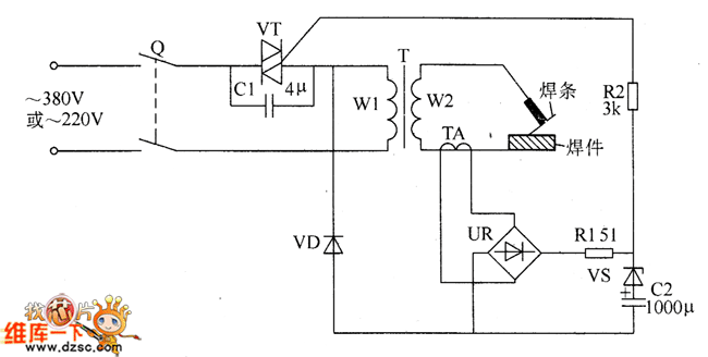
Description: The welder no-load power saver circuit consists of a current detection control circuit and a power saving control circuit, as illustrated in the accompanying chart. The current detection control circuit includes a current transformer (TA), a bridge rectifier (UR), a resistor (R1), a Zener diode (VS), a capacitor (C2), and a diode (VD). The power control circuit comprises additional resistors.
The welder no-load power saver circuit is designed to minimize energy consumption when the welder is not actively engaged in welding tasks. The current detection control circuit plays a crucial role in monitoring the current flowing through the welder. The current transformer (TA) is employed to sense the current and convert it into a proportional lower current suitable for processing.
The bridge rectifier (UR) converts the alternating current (AC) output from the current transformer into direct current (DC). This DC signal is then filtered and stabilized using the resistor (R1) and the Zener diode (VS), ensuring that the voltage remains within a specified range. The capacitor (C2) serves to smooth out any fluctuations in the rectified voltage, while the diode (VD) protects the circuit from reverse polarity.
The power saving control circuit is responsible for regulating the power supplied to the welder during idle periods. By utilizing resistors in this circuit, the system can effectively limit the power draw, thereby reducing overall energy consumption. This circuit operates in conjunction with the current detection control circuit to ensure that power is only consumed when necessary, thus enhancing the efficiency of the welder.
Overall, the welder no-load power saver circuit is an essential component for modern welding equipment, contributing to energy efficiency and operational cost savings. Its design incorporates various electronic components that work together to detect current usage and regulate power consumption, thereby providing a sustainable solution for welding applications.The welder no-load power saver circuit is composed of the current detection control circuit and power saving control circuit, and the circuit is shown as the chart. Current detection control circuit is composed of the current transformer TA, bridge rectifier UR, resistor R1, Zener diode VS, capacitor C2 and diode VD.
Power control circuit consists of resisto..
The welder no-load power saver circuit is designed to minimize energy consumption when the welder is not actively engaged in welding tasks. The current detection control circuit plays a crucial role in monitoring the current flowing through the welder. The current transformer (TA) is employed to sense the current and convert it into a proportional lower current suitable for processing.
The bridge rectifier (UR) converts the alternating current (AC) output from the current transformer into direct current (DC). This DC signal is then filtered and stabilized using the resistor (R1) and the Zener diode (VS), ensuring that the voltage remains within a specified range. The capacitor (C2) serves to smooth out any fluctuations in the rectified voltage, while the diode (VD) protects the circuit from reverse polarity.
The power saving control circuit is responsible for regulating the power supplied to the welder during idle periods. By utilizing resistors in this circuit, the system can effectively limit the power draw, thereby reducing overall energy consumption. This circuit operates in conjunction with the current detection control circuit to ensure that power is only consumed when necessary, thus enhancing the efficiency of the welder.
Overall, the welder no-load power saver circuit is an essential component for modern welding equipment, contributing to energy efficiency and operational cost savings. Its design incorporates various electronic components that work together to detect current usage and regulate power consumption, thereby providing a sustainable solution for welding applications.The welder no-load power saver circuit is composed of the current detection control circuit and power saving control circuit, and the circuit is shown as the chart. Current detection control circuit is composed of the current transformer TA, bridge rectifier UR, resistor R1, Zener diode VS, capacitor C2 and diode VD.
Power control circuit consists of resisto..

zener diode tester schematic
The electronic scheme provided can be used to design a Zener diode tester utilizing a few electronic components. This Zener tester, in conjunction with a multimeter, allows for the precise measurement of the threshold voltage of a Zener diode. The...

Capacitor Charger Lead Acid Battery
Leaving aside the complex chargers, "stuffed" electronics capacitor charger is one of the best connections. Charging current is limited by the resistor (or other element of the changing excess energy into heat), but the reactance of the capacitor to the...

Three Phase protective circuit of the current detection line
Drawing transistors that comprise the gate VTi, VT2, VT3, and similar components.
The schematic involves a configuration of transistors designated as VTi, VT2, and VT3, which are integral to forming a gate structure. These transistors are typically arranged in a complementary...

analog How to analyze this diode circuit
The two diodes will fail. It is advisable to include series resistors for them. If the simulation is successful, the current through the diodes will be excessive. Both diodes do not necessarily need to fail; one may become a Smoke...
Diode Matching Circuit
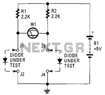
This circuit can be utilized to match diodes for applications where balance is essential, such as in a balanced modulator. The diode matching circuit will display the forward voltage drop of the two diodes in millivolts.
The diode matching circuit is...

Zener Diode Tester
Using a single 555 Timer IC and a small transformer to generate a high voltage, this circuit will test zener diodes of voltage ratings up to 50VDC. The 555 timer is used in the astable mode, the output at pin3...
diode radio circuit
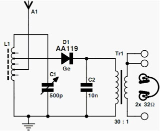
Currently, the most commonly available headphones have an impedance ranging from 2 to 32 ohms. This relatively low value renders them unsuitable for certain designs. However, with some clever modifications, these headphones can be effectively utilized in such applications. To...

Capacitor internal resistor meter
The design presented here works by applying a 50kHz, 200mV square wave to the capacitor under test, in series with a 10 Ohm resistor. The AC voltage appearing across that resistor is measured and displayed on a meter. So the...
Simple Diode Curve Tracer
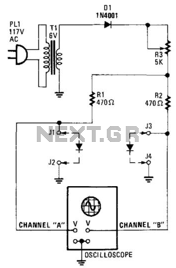
Suitable for matching diodes or examining the VI characteristics of two-terminal devices (such as diodes), this circuit is designed for laboratory use. Resistors R1 and R2 can be increased in value, and a higher voltage transformer can be utilized for...