


Fully Automatic Emergency Light circuit
#NE555
#LM317
#astable multivibrator
#Darlington pair
#emergency light
#timer
#voltage regulator
#squarewave
#transistor
#power supply

Description: The circuit consists of inverter and charger sections. The inverter section utilizes the NE555 timer, while the charger section is based on the LM317 adjustable regulator. In the inverter section, the NE555 is configured as an astable multivibrator, generating a 15kHz square wave. Output pin 3 of the NE555 is linked to a Darlington pair formed by the transistors SL100 (T1) and 2N3055 (T2) through resistor R4.
The inverter section of this circuit is designed to convert a DC input voltage into an AC output voltage. The NE555 timer, functioning as an astable multivibrator, continuously oscillates to produce a square wave signal at a frequency of 15 kHz. This square wave is crucial for driving the subsequent power amplification stage. The output from pin 3 of the NE555 is a square wave that toggles between high and low states, which is then amplified by the Darlington pair consisting of transistors SL100 and 2N3055. The Darlington configuration allows for high current gain, making it suitable for applications requiring substantial output power. The resistor R4 serves to limit the base current to the transistors, ensuring stable operation and preventing damage due to excessive current.
The charger section of the circuit is responsible for regulating the voltage supplied to a connected battery or load. The LM317 adjustable voltage regulator is employed for this purpose, allowing for precise control over the output voltage. The LM317 can provide a variable output voltage, typically ranging from 1.25V to 37V, depending on the external resistors used in the configuration. This flexibility makes the circuit suitable for various charging applications, accommodating different battery types and voltages.
Overall, this circuit effectively combines the inverter and charger functionalities, making it a versatile solution for powering AC loads while simultaneously providing a regulated DC charging capability. The design emphasizes efficiency and reliability, suitable for use in various electronic applications.The circuit can be divided into inverter and charger sections. The inverter section is built around timer NE555, while the charger section is built around 3-terminal adjustable regulator LM317. In the inverter section, NE555 is wired as an astable multivibrator that produces a 15kHz squarewave.
Output pin 3 of IC 555 is connected to the Darlington pair formed by transistors SL100 (T1) and 2N3055 (T2) via resistor R4..
The inverter section of this circuit is designed to convert a DC input voltage into an AC output voltage. The NE555 timer, functioning as an astable multivibrator, continuously oscillates to produce a square wave signal at a frequency of 15 kHz. This square wave is crucial for driving the subsequent power amplification stage. The output from pin 3 of the NE555 is a square wave that toggles between high and low states, which is then amplified by the Darlington pair consisting of transistors SL100 and 2N3055. The Darlington configuration allows for high current gain, making it suitable for applications requiring substantial output power. The resistor R4 serves to limit the base current to the transistors, ensuring stable operation and preventing damage due to excessive current.
The charger section of the circuit is responsible for regulating the voltage supplied to a connected battery or load. The LM317 adjustable voltage regulator is employed for this purpose, allowing for precise control over the output voltage. The LM317 can provide a variable output voltage, typically ranging from 1.25V to 37V, depending on the external resistors used in the configuration. This flexibility makes the circuit suitable for various charging applications, accommodating different battery types and voltages.
Overall, this circuit effectively combines the inverter and charger functionalities, making it a versatile solution for powering AC loads while simultaneously providing a regulated DC charging capability. The design emphasizes efficiency and reliability, suitable for use in various electronic applications.The circuit can be divided into inverter and charger sections. The inverter section is built around timer NE555, while the charger section is built around 3-terminal adjustable regulator LM317. In the inverter section, NE555 is wired as an astable multivibrator that produces a 15kHz squarewave.
Output pin 3 of IC 555 is connected to the Darlington pair formed by transistors SL100 (T1) and 2N3055 (T2) via resistor R4..

SINGLE TRANSISTOR CODE PRACTICE OSCILLATOR
A 2N366 is configured as an audio feedback oscillator using an audio transformer. Adjust R1 for proper operation and the desired audio note.
The circuit utilizes a 2N366 transistor, which is a general-purpose NPN transistor, serving as the primary active component...

With NE555 make double touch light switch 2
The circuit illustrated in the figure features a dashed line on the left, representing a standard lighting circuit, while the right side is responsible for the dual functionality of touch activation using the NE555 timer. Components VD1 through VD4 form...
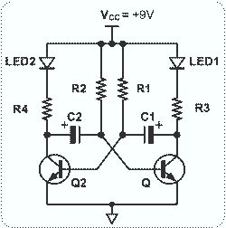
Astable Multivibrator with 2 Transistors
This circuit is straightforward and easy to construct, utilizing two transistors as active components along with several passive components such as resistors, capacitors, and two LEDs. The circuit employs the MPS2222 transistor, though any NPN type transistor can be used...

Transistorized Bar-Graph Driver
A resistor network (R1 through R10) with emitter followers (Q1 and Q2) drives LED drivers (Q3 through Q7). This circuit was utilized as a "light organ" to provide visual volume indication. It can be connected to a speaker, another audio...

STABILIZER POWER SUPPLY 0-30 VDC CIRCUIT
This is an aerial current power supply with a continuously adjustable stabilized output ranging from 0 to 30VDC. The circuit also incorporates an electronic current limiter that effectively controls the output current from a few milliamperes (2 mA) to a...

Emergency Light and Alarm circuit
This circuit is permanently connected to a mains socket and is designed for trickle charging nickel-cadmium (Ni-Cd) batteries. In the event of a power outage, the lamp automatically turns on. An alarm sounder can be used in place of the...

Sony KV-S29MHl TV switching power supply (SIR a 80145A) circuit diagram
The circuit of the Sony KV-S29MHl (S Movement series) TV switching power supply (SIR a 80145A) consists of three main sections: (A) the power oscillation part, (B) the regulator part, and (C) the output section.
The Sony KV-S29MHl TV switching power...

Alternating current voltage amplifier transistor
An alternating current voltage amplifier transistor AC path is described. In AC analysis, the internal resistance of the AC supply voltage source is low, which corresponds to a short circuit signal. Consequently, the alternating voltage terminal Vcc is considered to...

With NE555 making push-button delay section lamp circuit
The NE555 push-button delay lamp circuit is illustrated in Figure 3-5. This circuit features several components, including a power supply and relay control system. Typically, the switch SB and normally open relay contacts K1 are in an open state, which...