


how to build a100 watt pure sine wave
#pure sine wave
#inverter
#100 watt
#differential amplifier
#power electronics
#AC/DC conversion
#discrete components
#modifiable output

Description: The circuit presented in this article illustrates a straightforward method for constructing a compact inverter that is easy to assemble and offers the functionality of a pure sine wave inverter. The design can be easily modified to achieve higher output levels. The input stage, which consists of transistors T1 and T2, forms a discrete differential amplifier that enhances the low amplitude input signal from the sine generator. A significant drawback of sine wave inverters is the excessive heat generated by the output devices, which considerably diminishes the overall efficiency of the system. This design aims to reduce the current requirements of the circuit, thereby helping to keep the devices cooler and increasing the system's efficiency. Once implemented, this circuit ensures a clean, hassle-free pure sine wave output suitable for powering various electrical devices, including computers. Additionally, a power output stage utilizing MOSFETs is presented, which can be integrated with the aforementioned sine generator circuit to create a high-power pure sine wave inverter capable of delivering 150 watts.
The described inverter circuit is designed for simplicity and effectiveness, emphasizing the use of a discrete differential amplifier formed by transistors T1 and T2. This configuration serves to amplify the low-level sine wave signal generated by the sine generator, ensuring that the output maintains high fidelity. The choice of transistors is critical; they must be selected based on their frequency response and thermal characteristics to optimize performance and minimize heat generation.
To address the common issue of overheating in sine wave inverters, this design incorporates techniques to reduce current draw. This approach not only prolongs the lifespan of the components but also enhances the overall efficiency of the inverter. By minimizing thermal stress on the output devices, the inverter can operate more reliably under various load conditions.
The output stage, which employs MOSFETs, is tailored to handle higher power levels while maintaining the integrity of the sine wave output. MOSFETs are preferred for their fast switching capabilities and lower on-resistance, which contribute to reducing power losses and improving thermal management. The design allows for scalability, enabling modifications to increase the output power beyond the base 150 watts, depending on the application requirements.
This inverter circuit is versatile and can be utilized to power a wide range of electrical devices, making it suitable for both residential and commercial applications. Its ability to produce a clean sine wave output ensures compatibility with sensitive electronic equipment, including computers, which require stable power sources to operate effectively. Overall, this circuit design represents a practical solution for achieving efficient power conversion while addressing common challenges associated with sine wave inverters.The circuit provided in this article shows you a simple way of building a useful liitle inverter thats easy to build and yet provides the features of a pure sine wave inverter. The circuit can be easily modified for getting higher outputs. The input stage consisting of T1 and T2 form a discrete differential amplifier, responsible for boosting the
low amplitude input signal from the sine generator. As we all know that the biggest drawback with sine wave inverters is its RED HOT output devices, which drastically reduces the over all efficiency of the system. This will help to reduce the current requirements of the circuit and thus help to keep the devices cooler.
The approach will also help to increase the efficiency of the system. Once this is done, you can rest assured of a clean, hassle free pure sine wave output that may be used for powering ANY electrical gadget, even your computer. Another power output stage is shown below using MOSFETs, which may be used in conjunction with the above discussed sine generator circuit for making a 150 watts high power pure sine wave inverter.
The described inverter circuit is designed for simplicity and effectiveness, emphasizing the use of a discrete differential amplifier formed by transistors T1 and T2. This configuration serves to amplify the low-level sine wave signal generated by the sine generator, ensuring that the output maintains high fidelity. The choice of transistors is critical; they must be selected based on their frequency response and thermal characteristics to optimize performance and minimize heat generation.
To address the common issue of overheating in sine wave inverters, this design incorporates techniques to reduce current draw. This approach not only prolongs the lifespan of the components but also enhances the overall efficiency of the inverter. By minimizing thermal stress on the output devices, the inverter can operate more reliably under various load conditions.
The output stage, which employs MOSFETs, is tailored to handle higher power levels while maintaining the integrity of the sine wave output. MOSFETs are preferred for their fast switching capabilities and lower on-resistance, which contribute to reducing power losses and improving thermal management. The design allows for scalability, enabling modifications to increase the output power beyond the base 150 watts, depending on the application requirements.
This inverter circuit is versatile and can be utilized to power a wide range of electrical devices, making it suitable for both residential and commercial applications. Its ability to produce a clean sine wave output ensures compatibility with sensitive electronic equipment, including computers, which require stable power sources to operate effectively. Overall, this circuit design represents a practical solution for achieving efficient power conversion while addressing common challenges associated with sine wave inverters.The circuit provided in this article shows you a simple way of building a useful liitle inverter thats easy to build and yet provides the features of a pure sine wave inverter. The circuit can be easily modified for getting higher outputs. The input stage consisting of T1 and T2 form a discrete differential amplifier, responsible for boosting the
low amplitude input signal from the sine generator. As we all know that the biggest drawback with sine wave inverters is its RED HOT output devices, which drastically reduces the over all efficiency of the system. This will help to reduce the current requirements of the circuit and thus help to keep the devices cooler.
The approach will also help to increase the efficiency of the system. Once this is done, you can rest assured of a clean, hassle free pure sine wave output that may be used for powering ANY electrical gadget, even your computer. Another power output stage is shown below using MOSFETs, which may be used in conjunction with the above discussed sine generator circuit for making a 150 watts high power pure sine wave inverter.

12V Inverter Circuit Using 4013
This circuit diagram for a 12V inverter is simple to construct and utilizes inexpensive components that many electronics hobbyists may already possess. While it is feasible to create a more powerful circuit, the complexity arises from managing the significant currents...

50W Inverter 12VDC to 220VAC circuit diagram
The objective is to transmit additional information through the distribution of articles. Please contact us via email at [email protected] within 15 days if there are any issues related to article content, copyright, or other concerns. Prompt action will be taken...
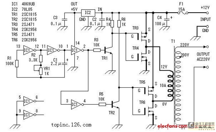
Circuit DIY of the inverter (picture and text is explained in detail)
The inverter described in this text utilizes a MOS field-effect transistor and a standard power transformer. Its output power is determined by the capabilities of both the MOS field-effect transistor and the transformer, eliminating the need for complex voltage transformer...

100Watt Inverter 24VDC to 220VAC II
This is a 100-watt inverter circuit diagram. It is built using the IC CD4047 and the MOSFET IRF540. This inverter has the capability to supply electronic devices that require 220VAC, with a maximum output of 100 watts from a 2-3A...

Switching (transformerless) DC/AC 12V/230V 150W modified sine wave inverter
The inverter is designed for powering mains appliances using battery sources. It functions as a switching converter, eliminating the need for bulky, heavy, and costly iron transformers. This design provides advantages such as compact size, lightweight construction, precise output voltage...

Using an inverter transistor monostable circuit diagram
The circuit diagram illustrates the connection of all three components of the series resonant crystal and triple CD4049 inverter. The supply voltage range is between 3 to 15 volts, making it suitable for various applications. This design is compact and...

And broadening the delay circuit
The inverter circuit using CD4069 is configured with a delay and width adjustment. When the output of the inverter (G1) is high, the capacitor (C) charges through resistor (R1) and diode (D). The voltage across capacitor C quickly reaches the...

Optional Flip inverter circuit
The circuit allows for the reversal or flipping of switch amplification without inversion. The voltage gain is dependent on the position of the switch, which can be either +1 or -1. There are two versions of the circuit, A and...

Discrete Voltage Regulator
The title of this article raises the question of why the extensive selection of fully integrated voltage regulators should be supplemented with a version built using discrete components. Specifically, what advantages does this circuit provide that the well-known three-terminal regulators...