


Switch-mode Converter Starts With Full Load Connected
#boost converter
#voltage regulation
#MOSFET
#gate-drive
#start-up circuit
#switching
#power electronics
#load management

Description: To ensure a full-load start-up, the additional circuitry in this regulated boost converter disconnects the load until the output voltage reaches regulation. Proper operation necessitates a gate-drive voltage adequate to maintain low on-resistance in the switching MOSFET; however, during start-up, this drive is restricted.
The regulated boost converter is designed to step up the input voltage to a higher output voltage while maintaining a stable output under varying load conditions. The additional circuitry plays a crucial role in managing the load connection during the start-up phase. By disconnecting the load until the output voltage stabilizes, the converter prevents potential damage to the load and ensures that the system operates within safe parameters.
The gate-drive voltage is a critical factor in the performance of the switching MOSFET. A sufficiently high gate-drive voltage is necessary to minimize the on-resistance of the MOSFET, which in turn reduces power losses and improves efficiency. During the start-up phase, the gate-drive voltage is intentionally limited to prevent excessive current draw, which could lead to instability or failure in the converter's operation.
Once the output voltage reaches the desired regulation level, the load is reconnected, allowing the converter to operate under full load conditions. This sequence ensures that the converter can handle the demands placed on it without compromising performance or reliability. The design of the control circuitry must take into account the timing and thresholds for disconnection and reconnection of the load, as well as the characteristics of the MOSFET and other components involved in the boost conversion process.
Overall, the regulated boost converter's design emphasizes safety and efficiency, particularly during the critical start-up phase, ensuring that it can deliver the required output voltage reliably under all operating conditions.To ensure a full-load start-up, the extra circuitry in this regulated boost converter disconnects the load until the output voltage achieves regulation. Proper operation requires a gate-drive voltage sufficient to provide low on-resistance in the switching MOSFET, but at start-up this drive is limited to the
The regulated boost converter is designed to step up the input voltage to a higher output voltage while maintaining a stable output under varying load conditions. The additional circuitry plays a crucial role in managing the load connection during the start-up phase. By disconnecting the load until the output voltage stabilizes, the converter prevents potential damage to the load and ensures that the system operates within safe parameters.
The gate-drive voltage is a critical factor in the performance of the switching MOSFET. A sufficiently high gate-drive voltage is necessary to minimize the on-resistance of the MOSFET, which in turn reduces power losses and improves efficiency. During the start-up phase, the gate-drive voltage is intentionally limited to prevent excessive current draw, which could lead to instability or failure in the converter's operation.
Once the output voltage reaches the desired regulation level, the load is reconnected, allowing the converter to operate under full load conditions. This sequence ensures that the converter can handle the demands placed on it without compromising performance or reliability. The design of the control circuitry must take into account the timing and thresholds for disconnection and reconnection of the load, as well as the characteristics of the MOSFET and other components involved in the boost conversion process.
Overall, the regulated boost converter's design emphasizes safety and efficiency, particularly during the critical start-up phase, ensuring that it can deliver the required output voltage reliably under all operating conditions.To ensure a full-load start-up, the extra circuitry in this regulated boost converter disconnects the load until the output voltage achieves regulation. Proper operation requires a gate-drive voltage sufficient to provide low on-resistance in the switching MOSFET, but at start-up this drive is limited to the

Mosfet 75W Power Amplifier
The MOSFETS we are dealing with are three terminal devices which are used to control electron flow in a circuit. Two of the pins (the source and drain) pass the current, and the third pin (the gate) is used to...

60w amplifier mosfet irfp240
The supply voltage rails were conservatively maintained at +40V and -40V. For those interested in experimentation, the supply voltage can be increased to a maximum of +50V and -50V, enabling the amplifier to reach its target output of 100W into...

Transistor Tutorial MOSFETs
The Metal-Oxide-Semiconductor Field-Effect Transistor (MOSFET) is analogous to the Junction Field-Effect Transistor (JFET) in several aspects. Both types are voltage-driven unipolar devices that rely on either electron or hole movement, but not both, unlike bipolar transistors. A key structural distinction...

Mosfet circuit schematics
Two working examples have been assembled, one utilizing a PNP and an NPN transistor, and the other employing two MOSFETs. Both circuits function correctly, but as anticipated, the MOSFET circuit draws significantly less current (0.1 mA compared to 4.5 mA)....
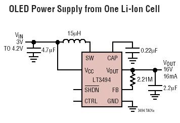
Micropower Low Noise Boost Converters with Output Disconnect
The LT3494 and LT3494A are low-noise boost converters that integrate a power switch, Schottky diode, and output disconnect circuitry. These devices utilize an innovative control technique that results in minimal output voltage ripple and high efficiency across a broad load...

100Khz-multiple-output-switching-power-supply
The power supply employs two VN4000A 400-V MOSPOWER FETs configured in a half-bridge arrangement. It provides outputs of +5 V at 20 A and ±15 V (or ±12 V) at 1 A. The low-current outputs utilize linear three-terminal regulators, allowing...

PC SMPS PWM chip CG8010DX16
This document contains the datasheet and the circuit diagram of a PC Switching Power Supply utilizing the IC CG8010DX16.
The CG8010DX16 is a highly integrated switching power supply controller designed for use in personal computer power supplies. It features a range...

100w basic mosfet amplifier
This basic MOSFET amplifier is simple to construct and low-cost, making it ideal for Hi-Fi amplifiers and instrument amplifiers such as guitars and keyboards. It delivers an output power of ±100 W RMS at an 8-ohm load or ±160 W...

MOSFET Power Amplifier
MOSFET Power Amplifier Circuit diagrams. Two complementary MOSFETs are used to deliver 20W into 8Ω.
The described MOSFET power amplifier circuit utilizes two complementary MOSFETs, which are arranged in a push-pull configuration to efficiently amplify audio signals. The circuit is designed...