


Simple light-operated street lamp circuit diagram(3)
#photodiode
#transistor
#thyristor
#street lamp
#light-operated
#resistance
#circuit
#automation
#sensor
#switch
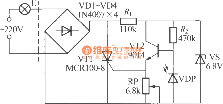
Description: The VDP is a photodiode that exhibits low resistance during the day, approximately 1 kΩ. As a result, transistor VT2 remains off, which keeps thyristor VT1 in the off-state due to the absence of trigger current at the gate, preventing the emitter (E) from being activated. At night, the photodiode shows high resistance due to the lack of light exposure, around 100 kΩ, causing VT2 to turn on and allowing the emitter to output a positive signal.
The circuit involves a photodiode (VDP) functioning as a light sensor, controlling the state of a transistor (VT2) and a thyristor (VT1). During daylight, the low resistance of the photodiode results in VT2 being non-conductive, which in turn ensures that VT1 remains off since there is no gate current to trigger it. Consequently, the emitter (E) does not receive power, thus remaining inactive.
In contrast, during nighttime, the photodiode's resistance increases significantly due to the absence of light, reaching approximately 100 kΩ. This high resistance activates VT2, allowing it to conduct. The activation of VT2 subsequently provides the necessary trigger current to the gate of thyristor VT1, turning it on. When VT1 is triggered, it allows current to flow to the emitter (E), resulting in its activation.
This configuration can be utilized in various applications, such as automatic lighting systems, where the circuit responds to ambient light levels. The transition between day and night conditions is critical for the operation of this circuit, ensuring that the emitter is only powered in low-light conditions. Proper selection of components, such as the photodiode, transistors, and thyristor, is essential to achieve the desired response times and sensitivity to light changes. The circuit may also include additional elements such as resistors for biasing and capacitors for filtering, which can enhance performance and stability.VDP is the photodiode and it has low resistance in the day, and resistance ? 1k?, then transistor VT2 is turned off, then thyristor VT1 is in the off-state as the gate has no trigger current, and E can not be lit. In the night, VL shows a high resistance as no light exposure, and the resistance ? 100k?, then VT2 is turned on, and the emitter can output pos..
The circuit involves a photodiode (VDP) functioning as a light sensor, controlling the state of a transistor (VT2) and a thyristor (VT1). During daylight, the low resistance of the photodiode results in VT2 being non-conductive, which in turn ensures that VT1 remains off since there is no gate current to trigger it. Consequently, the emitter (E) does not receive power, thus remaining inactive.
In contrast, during nighttime, the photodiode's resistance increases significantly due to the absence of light, reaching approximately 100 kΩ. This high resistance activates VT2, allowing it to conduct. The activation of VT2 subsequently provides the necessary trigger current to the gate of thyristor VT1, turning it on. When VT1 is triggered, it allows current to flow to the emitter (E), resulting in its activation.
This configuration can be utilized in various applications, such as automatic lighting systems, where the circuit responds to ambient light levels. The transition between day and night conditions is critical for the operation of this circuit, ensuring that the emitter is only powered in low-light conditions. Proper selection of components, such as the photodiode, transistors, and thyristor, is essential to achieve the desired response times and sensitivity to light changes. The circuit may also include additional elements such as resistors for biasing and capacitors for filtering, which can enhance performance and stability.VDP is the photodiode and it has low resistance in the day, and resistance ? 1k?, then transistor VT2 is turned off, then thyristor VT1 is in the off-state as the gate has no trigger current, and E can not be lit. In the night, VL shows a high resistance as no light exposure, and the resistance ? 100k?, then VT2 is turned on, and the emitter can output pos..

The counter
The circuit of this device is relatively straightforward. An input circuit filters the signal from the antenna to minimize sensitivity to other phenomena and protect against overvoltages. Four transistors create a "one-shot" section that is activated by the input circuit,...

Transistor act as a switch
A transistor is a semiconductor device utilized for switching and amplifying weak signals. This article details the operation of a transistor and its function as a switch. Currently, transistors are integrated into most electronic equipment for switching applications, with digital...
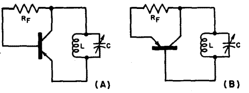
Fundamentals of Transistor Oscillators
This chapter discusses the operation and circuitry of transistor oscillators, which can be categorized into two types: feedback (similar to vacuum tube oscillators) and negative-resistance (current multiplying). Transistor oscillators can generate sine waves using various operational modes, including some novel...

Third harmonic excitation device automatic circuit a thyristor
The setup is connected to separate stator windings of a harmonic generator, which leads to a thyristor rectifier supply for the third harmonic voltage, positioned after the motor field. The output voltage varies with changes in the winding harmonics generator...

Bidirectional thyristor delay lamp circuit 2
Another method employs a Zhu gall thyristor delay lamp circuit. Typically, a 220V AC supply is used, consisting of a step-down voltage half-wave rectifier circuit. The circuit outputs approximately 25V across the left and right terminals. At this point, the...

Bedini SSG
The transistor activates, causing the magnet to move away. When the transistor deactivates, the energy stored in the coil collapses, directing its flow into the charging battery. As the next magnet approaches, the cycle repeats. This process effectively recaptures energy...

wireless fm transmitter
The wireless transmitter circuit utilizes transistor T1 (BF494) as a low-power variable-frequency VHF oscillator. A varicap diode circuit is incorporated to modify the frequency of the FM transmitter and to facilitate frequency modulation using audio signals. The output power of...
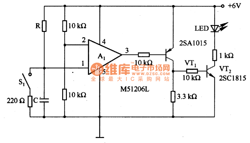
The time delay circuit diagram composed of transistor
The circuit is designed to set a delay time based on the voltage Us and the resistor R. In this configuration, S1 acts as the discharge switch for capacitor C. When switch S1 is closed, the stored charge in capacitor...

ECM Mic Preamplifier
Both transistors should be low-noise types. In the original circuit, BC650C was used, which is an ultra-low noise device. These transistors are now difficult to find, but BC549C or BC109C are good replacements. The circuit is self-stabilizing and will set...