


Automatic contrast meter
#photo-amplifier
#peak detectors
#sample and hold
#light intensity
#voltage measurement
#automatic contrast
#measurement circuit
#optical sensor

Description: The circuit arrangement includes a photo-amplifier that converts varying light levels in an enlarger into a voltage signal. This signal is processed by two peak detectors: one tracking the peak positive voltage and the other tracking the peak negative voltage. The capacitors that store the voltage peaks in the followers are also components of sample and hold circuits, which are activated to hold the values after measurement. The outputs of these circuits indicate the maximum and minimum light intensity levels. Subsequently, a differential amplifier calculates the ratio of these values, and the result is displayed on an LED bargraph meter.
The described circuit employs a photo-amplifier, which is essential for transforming the light intensity variations from an enlarger into a corresponding voltage signal. This voltage is then directed to two peak detectors, each designed to track specific voltage extremes: one for the highest (positive) peak and the other for the lowest (negative) peak. The use of capacitors in conjunction with these peak detectors serves a dual purpose. Not only do they store the detected voltage peaks, but they also contribute to the functionality of sample and hold circuits, which are crucial for capturing and maintaining the peak values during the measurement phase.
Upon completion of the measurement, the sample and hold circuits are activated to retain the stored voltages. The outputs from these circuits provide the maximum and minimum values of the light intensity, which are essential for further processing. The differential amplifier then takes these two outputs and computes their ratio, thereby providing a relative measure of the light intensity variations. This computed ratio is crucial for applications where precise light intensity control is required.
Finally, the result of the differential amplifier's computation is presented visually through an LED bargraph meter. This display method allows for immediate and intuitive interpretation of the light intensity levels, making it a practical solution for users who need to monitor light conditions in real-time. Overall, this circuit arrangement effectively integrates light sensing, voltage processing, and user-friendly output visualization, making it suitable for various applications in photography and optical measurements.The circuit arrangement consists of a photo-amplifier which feeds a voltage derived from varying light levels in an enlarger to a pair of peak detectors. One follows the peak positive voltage and the other the peak negative voltage. The capacitors used for storing the voltage peaks in the followers also form part of sample and hold circuits which are then switched to hold after the measurement.
Their outputs represent the maximum and minimum values of light intensity A differential amplifier then computes the ratio of these values, and the result is displayed on an LED bargraph meter.
The described circuit employs a photo-amplifier, which is essential for transforming the light intensity variations from an enlarger into a corresponding voltage signal. This voltage is then directed to two peak detectors, each designed to track specific voltage extremes: one for the highest (positive) peak and the other for the lowest (negative) peak. The use of capacitors in conjunction with these peak detectors serves a dual purpose. Not only do they store the detected voltage peaks, but they also contribute to the functionality of sample and hold circuits, which are crucial for capturing and maintaining the peak values during the measurement phase.
Upon completion of the measurement, the sample and hold circuits are activated to retain the stored voltages. The outputs from these circuits provide the maximum and minimum values of the light intensity, which are essential for further processing. The differential amplifier then takes these two outputs and computes their ratio, thereby providing a relative measure of the light intensity variations. This computed ratio is crucial for applications where precise light intensity control is required.
Finally, the result of the differential amplifier's computation is presented visually through an LED bargraph meter. This display method allows for immediate and intuitive interpretation of the light intensity levels, making it a practical solution for users who need to monitor light conditions in real-time. Overall, this circuit arrangement effectively integrates light sensing, voltage processing, and user-friendly output visualization, making it suitable for various applications in photography and optical measurements.The circuit arrangement consists of a photo-amplifier which feeds a voltage derived from varying light levels in an enlarger to a pair of peak detectors. One follows the peak positive voltage and the other the peak negative voltage. The capacitors used for storing the voltage peaks in the followers also form part of sample and hold circuits which are then switched to hold after the measurement.
Their outputs represent the maximum and minimum values of light intensity A differential amplifier then computes the ratio of these values, and the result is displayed on an LED bargraph meter.

EIGHT CHANNEL COMPUTERIZED 3SUP1 SUP SUB2 SUB DIGIT_VM
Displays up to eight different DC voltages on a CRT terminal of a microprocessor under keyboard control, using BASIC commands and a BASIC routine provided in the article. Utilizes a modified Motorola MC14433 dual-lamp integrating analog-to-digital converter. An unknown voltage...

Test-Measurement 4
In circuit diagrams provided in equipment manuals, voltages at various points in the circuit are typically indicated. A deviation from these specified values suggests that a component has failed and can help in identifying faulty areas. Specifications include: D.C. Voltage...
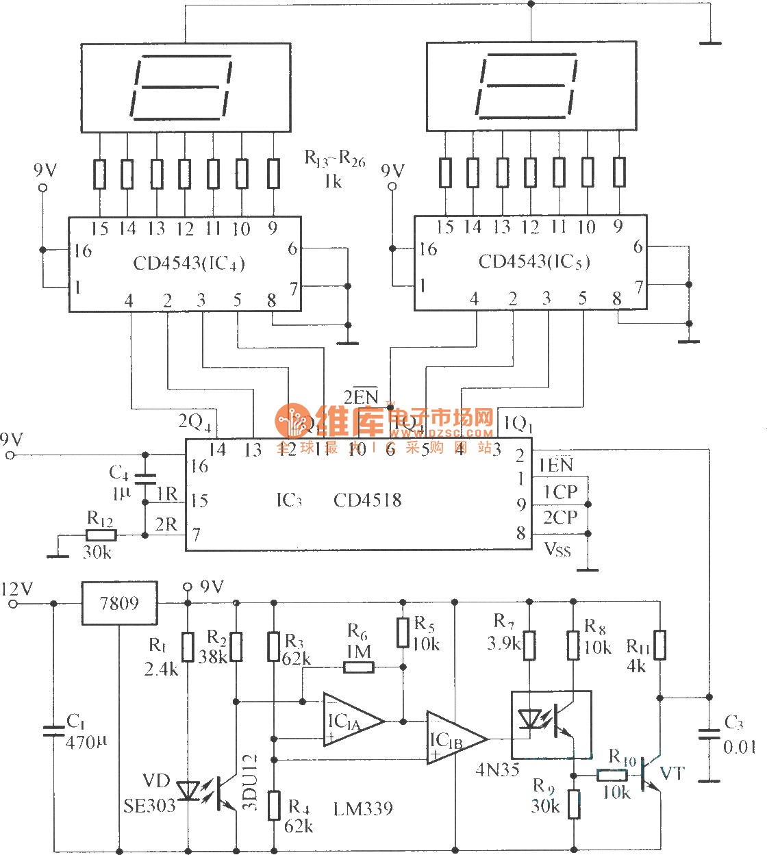
Digital displaying photoelectric counter circuit diagram
The circuit includes an optical input circuit (VD, 3DU12), a pulse forming circuit (IC1A, IC1B functioning as a voltage comparator; optical coupler; transistor switching circuit), and a counting and display circuit.
The circuit architecture consists of several key components that work...

Peak voltage sample and hold circuit
The peak voltage sample and hold circuit is illustrated in Figure 12-50. This circuit comprises the LF398 sample and hold chip and the LM311 voltage comparator. The LF398 is responsible for outputting and inputting voltages. The LM311 compares the input...
EIGHT CHANNEL COMPUTERIZED 3SUP1 SUP SUB2 SUB DIGIT_VM
Displays up to eight different DC voltages on a CRT terminal of a microprocessor under keyboard control, using BASIC commands and a BASIC routine provided in the article. Utilizes a modified Motorola MC14433 dual-lamp integrating analog-to-digital converter. An unknown voltage...

Infinite sample and hold amplifier
During normal hold mode, the replicated analog voltage is buffered directly through the sample-and-hold (S/H) amplifier to the output. Upon receiving a SAMPLE signal, the S/H amplifier enters hold mode, maintaining the voltage until the new analog voltage is valid....

High speed sample and hold
This circuit demonstrates a 10 V acquisition time of 900 ns with 0% accuracy and a droop rate of only 100 µV/ms at an ambient temperature of 25°C. A faster acquisition time can be achieved by using a smaller hold-capacitor...

Coulomb meter
Another cause of voltage drift is the input current of IC1, which slowly charges capacitor C1. This effect is particularly noticeable when the output voltage is approximately 0 volts.
The circuit in question involves an integrated circuit (IC1) whose input current...

Sample and hold
The JFETs, Q1 and Q2, provide complete buffering to C1, the sample and hold capacitor. During the sample phase, Q1 is activated, establishing a low-resistance path (rds(on)) for charging C1. In the hold phase, Q1 is deactivated, leaving Q1 Id...