


Creating Fast Line Transients
#transients
#integrated circuit
#power supply
#function generator
#measurement
#DUT
#bypass capacitor
#current requirements
#capacitance

Description: The response of an integrated circuit to fast transients on its input supply is a critical measurement. For micro-power devices that do not require an input bypass capacitor, a 50-ohm terminated function generator can be used to drive the power-supply input. However, as current requirements and capacitance increase, this method may yield unsatisfactory results. A viable solution for managing fast transients with large capacitive loads is to implement an open-loop buffer. An open-loop buffer, lacking feedback, remains insensitive to capacitive loads and can be engineered to meet various current requirements. Key specifications for this buffer include a high slew rate, substantial output drive capability, low offset voltage, minimal distortion, and thermal compensation. The accompanying circuit diagram meets these specifications and resembles a traditional BJT buffer with modifications. Since the transistors are not integrated on a single monolithic die, a bias adjustment mechanism is necessary, along with a method for maintaining constant bias under varying temperature conditions. The circuit comprises three primary sections: a high-impedance complementary input stage, a VBE multiplier for bias adjustment, and a complementary Darlington output stage. The input stage and VBE multiplier are powered by constant current sources, while the output stage receives bias from the VBE multiplier. Series resistors R7 and R8 connect the input stage to the VBE multiplier and output stage, allowing the VBE multiplier to manage output stage bias without conflicting with the input stage's bias levels. This consideration is crucial as the output stage generates heat due to load demands. Without these series resistors, the input stage could excessively bias the output stage at elevated temperatures. The VBE multiplier is mounted on the output heatsink, ensuring it thermally tracks the output stage and prevents thermal runaway. This circuit is designed for bipolar power supplies, operating approximately 5V above the maximum output and 5V below the minimum output, with +15V and -5V providing optimal performance. Multiple grounds are included on the board, and input supplies should utilize a short pair of heavy-gauge wires to the PCB, avoiding shared grounds with other circuitry. The output should connect to the DUT input with very short, heavy-gauge wires capable of carrying transient currents exceeding 10A. The buffer features a high input impedance to accommodate flexible drive requirements. It is important to avoid connecting the buffer's output to the DUT input without a driving signal present at the buffer's input. For output voltages under ±5V, a 50-ohm terminator should be placed directly at the buffer input. For output voltages up to 10V, the pulse generator can operate unterminated. Voltages exceeding this range will necessitate an external amplifier. The maximum supply voltage for the buffer is limited to |V+ - V-| < 40V.
An open-loop buffer circuit is essential for applications requiring rapid transient response, especially in environments with significant capacitive loads. The design employs a high-impedance input stage, which minimizes loading on the signal source while ensuring accurate signal reproduction. The VBE multiplier serves as an effective biasing mechanism, adjusting the bias current dynamically based on temperature variations. This feature is critical in maintaining consistent performance across a range of operating conditions.
The complementary Darlington output stage is designed to deliver high current gain, making it suitable for driving loads that require substantial current without sacrificing stability or introducing distortion. The inclusion of series resistors R7 and R8 is a strategic design choice that enhances the circuit's robustness by ensuring that the biasing of the output stage is not adversely affected by changes in the input stage's operating conditions. This design consideration is particularly important in high-power applications where thermal effects can significantly influence circuit performance.
The circuit's layout should prioritize short, direct connections for both power and signal paths to minimize inductance and resistance, which can degrade performance during transient events. The use of heavy-gauge wiring for connections that carry high transient currents is essential to prevent voltage drops and ensure reliable operation. Additionally, careful grounding practices should be observed to prevent ground loops and noise interference, which could compromise the integrity of the measurements taken with the buffer.
Overall, this open-loop buffer circuit is tailored for high-performance applications in electronic testing and measurement, where rapid response to transient signals is critical for accurate assessments of integrated circuit behavior.An integrated circuit`s response to fast transients on its input supply is often an important measurement to take. If the device under test (DUT) is a micro-power device and doesn`t require an input bypass capacitor, simply drive the power-supply input with a 50 © terminated function generator.
However, as the current requirements and capacitance are increased, this no longer provides acceptable results. One solution to obtaining this fast transient into large capacitive loads is to make an open-loop buffer. Because an open-loop buffer has no feedback, it is insensitive to capacitive loads and can be designed to meet most current requirements.
Important criteria for this buffer include high slew rate, high output drive, low offset voltage, low distortion, and thermal compensation. The circuit in the figure below satisfies these requirements. It is similar to the classic BJT buffer with a few modifications. Because the transistors used are not on a single monolithic die, some means has to be provided to adjust the bias.
Furthermore, the circuit must have some method to keep this bias constant over temperature. The circuit consists of three major blocks. There is a high-impedance complementary input stage, followed by a VBE multiplier for bias adjustment, and then a complementary Darlington output stage. The input stage and the VBE multiplier are biased with constant current sources, whereas the output stage is biased by the output of the VBE multiplier.
The key to connecting the input stage to the VBE multiplier and the output stage is the inclusion of some series resistance via resistors R7 and R8. This allows the VBE multiplier to control the output stage bias without fighting the bias levels of the input stage.
This becomes a factor as the output stage heats up due to load requirements. If the series resistors were not included, the input stage would overbias the output stage at elevated temperatures. Because the VBE multiplier is mounted on the output heatsink, it thermally tracks the output stage, eliminating thermal runaway.
This circuit is designed for bipolar power supplies above the maximum output by about 5V and below the minimum output by about 5V. Operation at +15V and -5V provides good performance. Note that multiple grounds have been included on the board. The input supplies should use a short pair of heavy-gauge wire to the PCB. Do not share these grounds with any other circuitry. The output should be connected to the DUT input with very short heavy-gauge wires. These wires will carry transient currents in excess of 10A and should be sized accordingly. The buffer was designed with a high input impedance to have flexible drive requirements. Don`t connect the output of the buffer to the input of the DUT without a driving signal on the buffer input.
If the output voltages are under ±5V, use a 50 © terminator right at the buffer input. If the output is up to 10V, run the pulse generator unterminated to get this voltage. Voltages beyond this will require the addition of an external amplifier. The maximum supply voltages for the buffer are |V+ - V-| < 40V.
An open-loop buffer circuit is essential for applications requiring rapid transient response, especially in environments with significant capacitive loads. The design employs a high-impedance input stage, which minimizes loading on the signal source while ensuring accurate signal reproduction. The VBE multiplier serves as an effective biasing mechanism, adjusting the bias current dynamically based on temperature variations. This feature is critical in maintaining consistent performance across a range of operating conditions.
The complementary Darlington output stage is designed to deliver high current gain, making it suitable for driving loads that require substantial current without sacrificing stability or introducing distortion. The inclusion of series resistors R7 and R8 is a strategic design choice that enhances the circuit's robustness by ensuring that the biasing of the output stage is not adversely affected by changes in the input stage's operating conditions. This design consideration is particularly important in high-power applications where thermal effects can significantly influence circuit performance.
The circuit's layout should prioritize short, direct connections for both power and signal paths to minimize inductance and resistance, which can degrade performance during transient events. The use of heavy-gauge wiring for connections that carry high transient currents is essential to prevent voltage drops and ensure reliable operation. Additionally, careful grounding practices should be observed to prevent ground loops and noise interference, which could compromise the integrity of the measurements taken with the buffer.
Overall, this open-loop buffer circuit is tailored for high-performance applications in electronic testing and measurement, where rapid response to transient signals is critical for accurate assessments of integrated circuit behavior.An integrated circuit`s response to fast transients on its input supply is often an important measurement to take. If the device under test (DUT) is a micro-power device and doesn`t require an input bypass capacitor, simply drive the power-supply input with a 50 © terminated function generator.
However, as the current requirements and capacitance are increased, this no longer provides acceptable results. One solution to obtaining this fast transient into large capacitive loads is to make an open-loop buffer. Because an open-loop buffer has no feedback, it is insensitive to capacitive loads and can be designed to meet most current requirements.
Important criteria for this buffer include high slew rate, high output drive, low offset voltage, low distortion, and thermal compensation. The circuit in the figure below satisfies these requirements. It is similar to the classic BJT buffer with a few modifications. Because the transistors used are not on a single monolithic die, some means has to be provided to adjust the bias.
Furthermore, the circuit must have some method to keep this bias constant over temperature. The circuit consists of three major blocks. There is a high-impedance complementary input stage, followed by a VBE multiplier for bias adjustment, and then a complementary Darlington output stage. The input stage and the VBE multiplier are biased with constant current sources, whereas the output stage is biased by the output of the VBE multiplier.
The key to connecting the input stage to the VBE multiplier and the output stage is the inclusion of some series resistance via resistors R7 and R8. This allows the VBE multiplier to control the output stage bias without fighting the bias levels of the input stage.
This becomes a factor as the output stage heats up due to load requirements. If the series resistors were not included, the input stage would overbias the output stage at elevated temperatures. Because the VBE multiplier is mounted on the output heatsink, it thermally tracks the output stage, eliminating thermal runaway.
This circuit is designed for bipolar power supplies above the maximum output by about 5V and below the minimum output by about 5V. Operation at +15V and -5V provides good performance. Note that multiple grounds have been included on the board. The input supplies should use a short pair of heavy-gauge wire to the PCB. Do not share these grounds with any other circuitry. The output should be connected to the DUT input with very short heavy-gauge wires. These wires will carry transient currents in excess of 10A and should be sized accordingly. The buffer was designed with a high input impedance to have flexible drive requirements. Don`t connect the output of the buffer to the input of the DUT without a driving signal on the buffer input.
If the output voltages are under ±5V, use a 50 © terminator right at the buffer input. If the output is up to 10V, run the pulse generator unterminated to get this voltage. Voltages beyond this will require the addition of an external amplifier. The maximum supply voltages for the buffer are |V+ - V-| < 40V.
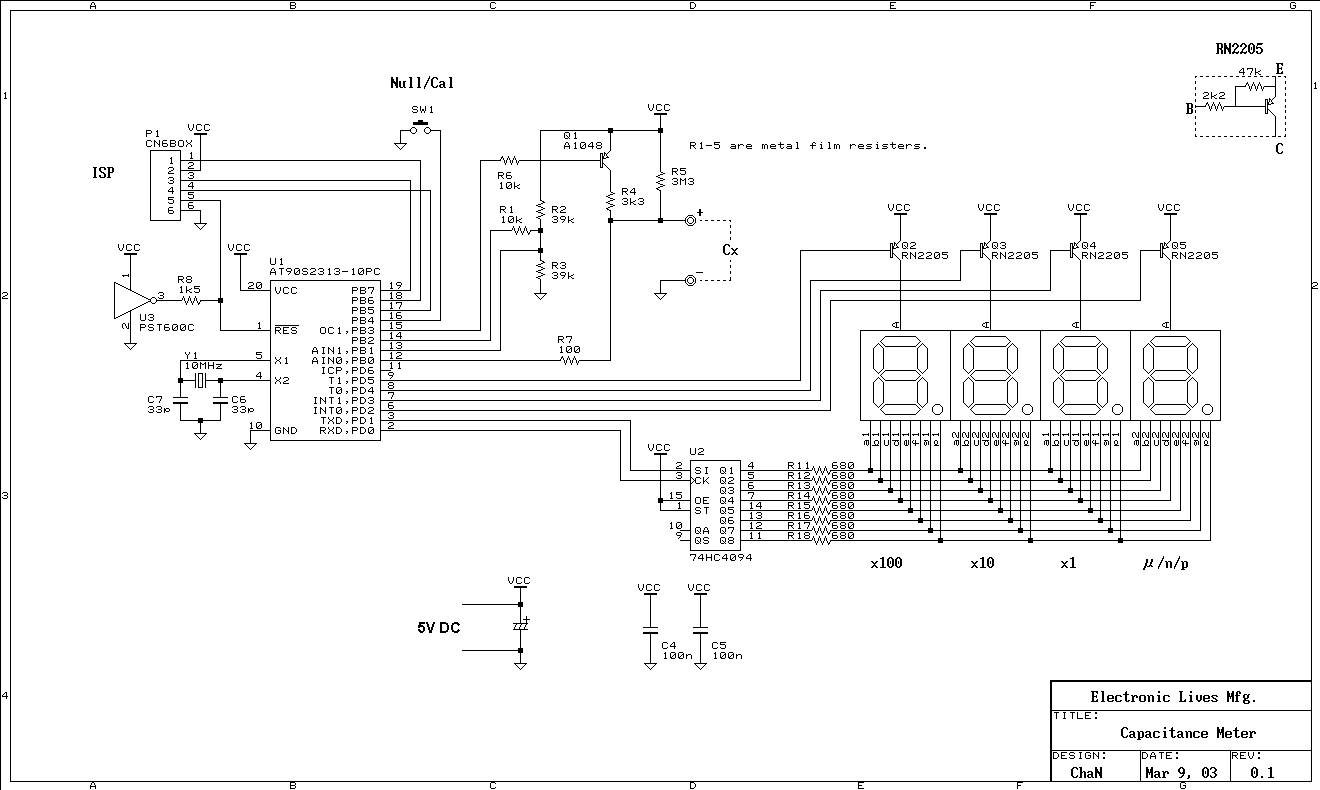
Digital Capacitance Meter
This is a simple capacitance meter which can measure capacitance value easy. There are some measurement methods for capacitance, at one time the capacitance was measured with a impedance bridge or a dip meter. Recently typical capacitance meters can measure...

20MHz High Speed Function Generator
The High Speed Function Generator was published in the professional electronics section of the Aug 1996 issue of Electronics Australia, and has proven to be extremely popular. The kit is no longer available from any of the kit suppliers.
The High...

FUNCTION GENERATOR
The circuit has both square-wave and triangle-wave output. The left section is similar in function to a comparator circuit that uses positive feedback for hysteresis. The inverting input is biased at one-half the Vcc voltage by resistor R4 and R5....

Two-Sheets Detector
This circuit utilizes the principle of capacitance between two plates to detect when multiple sheets of paper are placed between the sensing electrodes simultaneously. CI is the sensing capacitor, composed of two plates measuring 2 inches by 15 inches with...
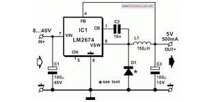
Switch Mode Power Supply
National Semiconductor has been producing and designing integrated circuits (ICs) for use in switch-mode power supplies for many years. The application of these devices is standard.
National Semiconductor has established a significant presence in the design and manufacturing of integrated circuits...

AMPLIFIER WITH FORCED EQUILIBRIUM ADAPTOR
Each power supply, whether linear or switching, operates in at least two modes: constant voltage (CV) and constant current (CC). The power supply can function in either mode, with the other serving as a protective mode for both the load...

Function Generators
A function generator is a signal source capable of producing various types of waveforms as its output signal. The most common output waveforms include sine waves, triangular waves, square waves, and sawtooth waves. The frequencies of these waveforms can be...

car battery charger schematics
The circuit is designed to be powered directly by a power supply, which is why it does not include a transformer, rectifier, or filter capacitors in the schematic. However, the addition of these components is possible. To operate the circuit,...

Audio Function Generator
Using an EXAR XR2206, this generator will produce sine, square, and triangular waves from 10 Hz to 100 kHz. The XR2206 chip, R7 controls frequency, and S5 through S8 select the frequency range. U3 produces a TTL-compatible square-wave output, while...