


Electrical modeling of a nanopore measurement
#nanopore
#current preamplifier
#low-noise
#voltage-clamp
#single-molecule
#impedance
#solid-state
#transient current
#feedback resistance
#circuit design

Description: An illustration of the electronic impedances of a solid-state nanopore chip. A simplified circuit schematic of the voltage-clamp current preamplifier is provided. The circuit design of the low-noise current source substitutes for a feedback resistance (RF). An example transient current pulse is shown, characteristic of a single-molecule event. The dominant sources of noise power spectral density are illustrated as a function of frequency. The platform concept was developed by J. K. R., K. L. S., and M. D. The amplifier and measurement system were designed by J. K. R. Experiments were planned by J. K. R., K. L. S., M. W., and M. D. Nanopores were fabricated by M. W. and C. A. M. Nanopore experiments and data analysis were performed by J. K. R. and M. W. The manuscript was written by J. K. R. and K. L. S., with contributions from all authors.
The electronic impedances of a solid-state nanopore chip play a crucial role in its functionality, particularly in applications such as DNA sequencing and single-molecule detection. The voltage-clamp current preamplifier is a vital component of the circuit schematic, designed to maintain a stable voltage across the nanopore while measuring the resulting current fluctuations. This configuration allows for precise control and measurement of ionic currents that occur as molecules pass through the nanopore.
The low-noise current source included in the design serves as a replacement for a feedback resistance (RF), which is essential to minimize the impact of thermal and electronic noise on the measurements. By employing a low-noise current source, the system can achieve higher sensitivity and accuracy in detecting transient current pulses that are indicative of single-molecule events. These pulses are characterized by their amplitude and duration, which provide information about the size and translocation speed of the molecules.
Additionally, the noise power spectral density is a critical parameter, illustrated as a function of frequency. Understanding the dominant sources of noise helps in optimizing the design and operation of the nanopore chip, ensuring that the signal-to-noise ratio is maximized for effective detection and analysis.
The collaborative efforts of the research team, including the design of the amplifier, planning of experiments, fabrication of nanopores, and analysis of data, highlight the interdisciplinary nature of this work. The manuscript detailing these findings reflects the collective contributions of all authors involved in the project, emphasizing the importance of teamwork in advancing the field of solid-state nanopore technology.An illustration of the electronic impedances of a solid-state nanopore chip. (b) Simplified circuit schematic of the voltage-clamp current preamplifier. (c) Circuit design of the low-noise current source that substitutes for a feedback resistance (RF). (d) An example transient current pulse, characteristic of a single-molecule event such as th e one illustrated. (e) Dominant sources of noise power spectral density, illustrated as a function of frequency. J. K. R. , K. L. S. and M. D. developed the platform concept. J. K. R. designed the amplifier and measurement system. J. K. R. , K. L. S. , M. W. and M. D. planned experiments. M. W. and C. A. M. fabricated nanopores. J. K. R. and M. W. performed nanopore experiments and analyzed data. J. K. R. and K. L. S. wrote the manuscript. All authors edited the manuscript.
The electronic impedances of a solid-state nanopore chip play a crucial role in its functionality, particularly in applications such as DNA sequencing and single-molecule detection. The voltage-clamp current preamplifier is a vital component of the circuit schematic, designed to maintain a stable voltage across the nanopore while measuring the resulting current fluctuations. This configuration allows for precise control and measurement of ionic currents that occur as molecules pass through the nanopore.
The low-noise current source included in the design serves as a replacement for a feedback resistance (RF), which is essential to minimize the impact of thermal and electronic noise on the measurements. By employing a low-noise current source, the system can achieve higher sensitivity and accuracy in detecting transient current pulses that are indicative of single-molecule events. These pulses are characterized by their amplitude and duration, which provide information about the size and translocation speed of the molecules.
Additionally, the noise power spectral density is a critical parameter, illustrated as a function of frequency. Understanding the dominant sources of noise helps in optimizing the design and operation of the nanopore chip, ensuring that the signal-to-noise ratio is maximized for effective detection and analysis.
The collaborative efforts of the research team, including the design of the amplifier, planning of experiments, fabrication of nanopores, and analysis of data, highlight the interdisciplinary nature of this work. The manuscript detailing these findings reflects the collective contributions of all authors involved in the project, emphasizing the importance of teamwork in advancing the field of solid-state nanopore technology.An illustration of the electronic impedances of a solid-state nanopore chip. (b) Simplified circuit schematic of the voltage-clamp current preamplifier. (c) Circuit design of the low-noise current source that substitutes for a feedback resistance (RF). (d) An example transient current pulse, characteristic of a single-molecule event such as th e one illustrated. (e) Dominant sources of noise power spectral density, illustrated as a function of frequency. J. K. R. , K. L. S. and M. D. developed the platform concept. J. K. R. designed the amplifier and measurement system. J. K. R. , K. L. S. , M. W. and M. D. planned experiments. M. W. and C. A. M. fabricated nanopores. J. K. R. and M. W. performed nanopore experiments and analyzed data. J. K. R. and K. L. S. wrote the manuscript. All authors edited the manuscript.

Low-noise preamplifier circuit
Low-noise preamplifier circuit. This circuit demonstrates a typical low-noise preamplifier design, which can be utilized to amplify signals from sources such as magnetic heads and microphones within audio applications. The input signal is coupled through a capacitor and subsequently passed...
High Power Solid State Amplifier
Building a solid-state linear amplifier. An old Heathkit SB 221 has undergone a major overhaul and redesign, and is now functioning well on 80, 40, 20, and 15 meters; however, it does not operate on 17, 12, and 10 meters....

Electronic Projects
This program includes circuit design CAD, simulation, and auto-routing PC layout. PSPICE is also utilized at Unisys, which offers more capabilities but costs six times as much and requires annual renewal. With these requirements and others in mind, a variation...

Solid-State Windshield-Wiper Delay
In the wiper-delay schematic presented, when the ignition is activated, Di maintains a regulated +12 V DC. Upon closing SI, CI bypasses transients and allows this +12 V DC to reach the resistor divider R2-R3, generating a TTL high signal...
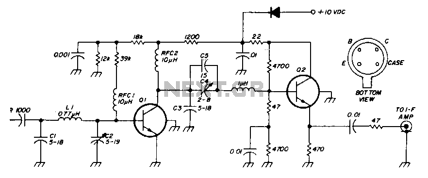
Low-noise 30Mhz preamplifier
The low-noise preamplifier features a noise figure of 1 dB at 30 MHz and a 3 dB bandwidth of 10 MHz. The gain is 19 dB. The total current drain with a +10 volt supply is 13 mA. The resistors...

Low-Noise Audio Preamp
A low-noise LT1115 (Linear Technology, Inc.) operational amplifier is connected to a class-A buffer amplifier to create a variable gain (12-to-50 dB) microphone preamplifier. Total harmonic distortion (THD) is less than 0.01% across a frequency range from 80 Hz to...

For low-noise amplifier OP amplifier RIAA compensation
A common telecoil follows the MM formula (magnetic-acting) and has an impedance of approximately 600 ohms to effectively receive signals. It is necessary to reduce the impedance in the high-frequency segment, which is achieved by placing a 150pF capacitor in...

Low-noise broadband amplifier
The amplifier delivers a gain of 10 dB across a frequency range of 10-600 MHz and features a 1-to-1 impedance match at 50 ohms. The BFR91 transistor exhibits a noise figure of 1 dB at 500 MHz. The circuit operates...
Low-noise preamplifier circuit
Low-noise preamplifier circuit. This circuit demonstrates a typical low-noise preamplifier design, which can be utilized to amplify signals from sources such as magnetic heads and microphones within audio applications. The input signal is coupled through a capacitor and subsequently passed...