


Solid laser range finder reception circuit
#laser range finder
#amplifier
#bandwidth
#input resistance
#output resistance
#noise level
#direct coupling amplifier
#negative feedback
#Zener diode

Description: The amplification of this circuit is approximately 12,000 times, with a bandwidth ranging from 0.5 to 14 MHz. The input resistance is 700 ohms, while the output resistance is 35 ohms (measured at 5 MHz). The output noise level is between 0.6 and 0.8 volts. In the schematic, transistors T1 and T2 function as direct coupling amplifiers, configured with parallel current negative feedback. The Zener diode 2CW11 enhances the emitter level of T2.
This circuit exemplifies a high-gain amplifier designed for applications requiring significant signal amplification with a wide bandwidth. The gain of 12,000 indicates that the circuit is suitable for low-signal applications, where even minute input signals can be amplified to usable levels. The specified bandwidth of 0.5 to 14 MHz suggests that the circuit can handle a variety of signal frequencies, making it versatile for different electronic applications.
The input resistance of 700 ohms is relatively high, allowing for minimal loading on the preceding stage, which is crucial in maintaining signal integrity. Conversely, the output resistance of 35 ohms, measured at 5 MHz, indicates a low output impedance, which is beneficial for driving subsequent stages or loads without significant loss of signal strength.
The direct coupling configuration of transistors T1 and T2 allows for efficient signal transfer between stages without the need for coupling capacitors, which can introduce phase shifts and frequency response issues. The parallel current negative feedback employed in this design stabilizes the gain and improves linearity, thus reducing distortion and enhancing overall performance.
The inclusion of the Zener diode 2CW11 serves a critical role in regulating the emitter voltage of transistor T2, ensuring that the transistor operates within its optimal range. This regulation helps to maintain consistent performance across varying operating conditions and contributes to the stability of the amplifier.
Overall, this circuit design is well-suited for applications in audio amplification, RF signal processing, and other areas where high gain and low noise are essential.The amplification of this circuit is about 12000 times, the bandwidth is 0.5~14MHz, the input resistance is 700?, the output resistance is 35?(measured with 5MHz), the output noise level is 0.6~0.8V. In figure, T1, T2 are direct coupling amplifier, they are connected into parallel current negative feedback.
Zener diode 2CW11 improves T2 emitter level, i..
This circuit exemplifies a high-gain amplifier designed for applications requiring significant signal amplification with a wide bandwidth. The gain of 12,000 indicates that the circuit is suitable for low-signal applications, where even minute input signals can be amplified to usable levels. The specified bandwidth of 0.5 to 14 MHz suggests that the circuit can handle a variety of signal frequencies, making it versatile for different electronic applications.
The input resistance of 700 ohms is relatively high, allowing for minimal loading on the preceding stage, which is crucial in maintaining signal integrity. Conversely, the output resistance of 35 ohms, measured at 5 MHz, indicates a low output impedance, which is beneficial for driving subsequent stages or loads without significant loss of signal strength.
The direct coupling configuration of transistors T1 and T2 allows for efficient signal transfer between stages without the need for coupling capacitors, which can introduce phase shifts and frequency response issues. The parallel current negative feedback employed in this design stabilizes the gain and improves linearity, thus reducing distortion and enhancing overall performance.
The inclusion of the Zener diode 2CW11 serves a critical role in regulating the emitter voltage of transistor T2, ensuring that the transistor operates within its optimal range. This regulation helps to maintain consistent performance across varying operating conditions and contributes to the stability of the amplifier.
Overall, this circuit design is well-suited for applications in audio amplification, RF signal processing, and other areas where high gain and low noise are essential.The amplification of this circuit is about 12000 times, the bandwidth is 0.5~14MHz, the input resistance is 700?, the output resistance is 35?(measured with 5MHz), the output noise level is 0.6~0.8V. In figure, T1, T2 are direct coupling amplifier, they are connected into parallel current negative feedback.
Zener diode 2CW11 improves T2 emitter level, i..

Amplifier circuit
An amplifier is a device that accepts a varying input signal and produces an output signal that varies in the same way as the input but has a larger amplitude. The input signal may be a current, voltage, mechanical motion,...

OCL AC negative feedback amplifier analysis
The AC negative feedback circuit consists of resistors R and R, as illustrated in Figure 1-30. In this configuration, capacitor C3 can be treated as a short circuit. The actual results are depicted in Figure 1-32. An AC voltage series...

Broadband high frequency amplifying circuit
A broadband high-frequency amplifying circuit is primarily composed of a high-frequency matching transformer and an amplifying transistor. This circuit is designed to handle large high-frequency signals. The input of the amplifier circuit utilizes a matching transformer to ensure that the...

KA9270 Audio Filter Introduction
KGA8010 is a broadband distributed amplifier utilizing 0.1 um-gate GaAs P-HEMT and coplanar waveguide technologies. The KGA8010 can serve as a multi-purpose amplifier for 40 Gb/s optical communication and millimeter wave applications. Manufactured by Oki Semiconductor.
The KGA8010 broadband distributed amplifier...

Zener Oscillator circuits
These two circuits are interesting from an academic point of view. Their practical implementation is rather critical and it is not easy to get steady operation. Circuit (a) requires a "cooked" zener: connect it first to a constant current generator,...
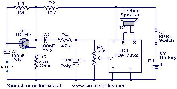
Speech amplifier circuit
This circuit can be housed within a box containing a speaker to create a convenient microphone amplifier. It is suitable for use by teachers, guides, lecturers, and others in crowded or noisy environments. The design is based on the audio...

Zener diode increase regulator output
A zener diode in the ground lead of a fixed PNP regulator varies the voltage output of that device without a significant sacrifice in regulation. The technique also allows the regulator to operate with output voltages beyond its rated limit.
The...

Active-limiting-amplifier
The modified inverting amplifier employs an active clamp to precisely limit the output swing. Consideration must be given to the VBE of the transistors. The output swing is restricted by the base-emitter breakdown of the transistors. A straightforward circuit configuration...

DC-Coupled Audio Amplifier circuit
Designs for audio amplifiers with DC coupling to the load are not frequently seen today, despite offering distinct advantages.
Audio amplifiers that employ DC coupling to the load provide several benefits that can enhance performance in specific applications. In traditional audio...