


display board to interface it with 8051
Description: 74hc573 is used to store data so that the previous content on SS is not vanish when we disable LE pin. T0 select the proper latch 74hc238, 3x8 decoder is used. And to convert BCD into decimal, 74ls48 converter is used. Note that latches U1 to U4 are connected with C.C SS, so the output of 74ls48 will only go to these latches. Whereas latches U6 and U8 are connected to DP oF SS and LEDs respectfully. You can emit these latches i used them to distinguish between various mode i.e, digital clock, stop watch, counter and manual input. 8051 Generic Board is my fist project board in 8051 microcontroller course. This board is design for atmel 89c51 ic, please refer to its datasheet for more information.
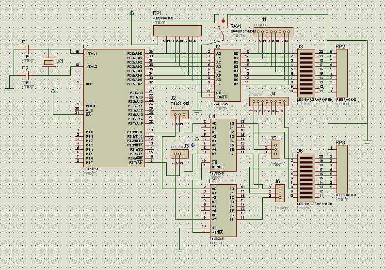
Now come towards board description: There are four i/o ports in 89c51, this board is design in such a manner that all ports are byte addressable whare as port3 can also be access bit wise in other world port 3 is also bit addressable. This can be done by proper selecting the jumper j2 and j5 and etc.Note that there are 8 jumpers at port 3 and also 8 jumpers at the u4 & u5 o/p pins are required, whereas in schematic only four are shown.
74ls245 latches are used to decide the direction of data. Switch SW1 is used to select the direction. If SW1 is towards vcc than the data direction is from 89c51 to latch o/p pins. And if SW1 is towards gnd than the direction is from latch to 89c51. For more info please refer to its datasheet.
LED bargraph are used to indicate the status of 89c51 port pins; that is data in or out. Connectors J1, J4 and etc are used so that we can interface this board with other boards. Note that only port 0 and port 3 connections are shown in schematic; port 1 and port 2 connection are the same as of port 0, but in that case RP1 is not required. As port 0 needs to be pull up so, resistor pack, RP1, is only required for this port.
The circuit utilizes a 74HC573 octal latch to maintain data integrity on the SS signal line, ensuring that data is preserved even when the LE (Latch Enable) pin is disabled. The 74HC238, a 3-to-8 line decoder, is employed to select the appropriate latch for data storage. Additionally, a 74LS48 BCD to decimal decoder is incorporated to convert binary-coded decimal inputs into decimal outputs. The outputs from the 74LS48 are directed to latches U1 to U4, which are specifically connected to the common SS line, while latches U6 and U8 interface with the decimal point (DP) of the SS and the LED indicators, respectively. This configuration allows the system to operate in various modes, including digital clock, stopwatch, counter, and manual input.
The board is designed for the Atmel 89C51 microcontroller, featuring four I/O ports. Each port is byte-addressable, with Port 3 configured for bit-addressable access. This flexibility is achieved through the appropriate selection of jumpers (J2, J5, etc.). The schematic representation includes eight jumpers for Port 3, with additional jumpers for output pins at U4 and U5, although only four are depicted in the schematic.
Data direction is controlled by the 74LS245 latches, with a switch (SW1) determining the flow of data. When SW1 is connected to VCC, data flows from the 89C51 to the latch output pins. Conversely, when SW1 is connected to GND, the data direction reverses, allowing data to flow from the latches back to the 89C51. The LED bar graph serves as a visual indicator of the status of the 89C51 port pins, showing whether data is being input or output.
Connectors such as J1 and J4 facilitate interfacing with other boards, ensuring compatibility and expandability. It is important to note that while the schematic shows connections for Port 0 and Port 3, Ports 1 and 2 share the same connection scheme as Port 0, with the exception that a resistor pack (RP1) is only necessary for Port 0 to provide the required pull-up resistors.74hc573 is used to store data so that the previous content on SS is not vanish when we disable LE pin. T0 select the proper latch 74hc238, 3x8 decoder is used. And to convert BCD into decimal, 74ls48 converter is used. Note that latches U1 to U4 are connected with C.C SS, so the output of 74ls48 will only go to these latches.
Whereas latches U6 and U8 are connected to DP oF SS and LEDs respectfully. You can emit these latches i used them to distinguish between various mode i.e, digital clock, stop watch, counter and manual input... 8051 Generic Board is my fist project board in 8051 microcontroller course. This board is design for atmel 89c51 ic, please refer to its datasheet for more information. Now come towards board description: There are four i/o ports in 89c51, this board is design in such a manner that all ports are byte addressable whare as port3 can also be access bit wise in other world port 3 is also bit addressable. This can be done by proper selecting the jumper j2 and j5 and etc.Note that there are 8 jumpers at port 3 and also 8 jumpers at the u4 & u5 o/p pins are required, whereas in schematic only four are shown.
74ls245 latches are used to decide the direction of data. Switch SW1 is used to select the direction. If SW1 is towards vcc than the data direction is from 89c51 to latch o/p pins. And if SW1 is towards gnd than the direction is from latch to 89c51. For more info please refer to its datasheet. LED bargraph are used to indicate the status of 89c51 port pins; that is data in or out. Connectors J1, J4 and etc are used so that we can interface this board with other boards. Note that only port 0 and port 3 connections are shown in schematic; port 1 and port 2 connection are the same as of port 0, but in that case RP1 is not required. As port 0 needs to be pull up so, resistor pack, RP1, is only required for this port.
Now come towards board description: There are four i/o ports in 89c51, this board is design in such a manner that all ports are byte addressable whare as port3 can also be access bit wise in other world port 3 is also bit addressable. This can be done by proper selecting the jumper j2 and j5 and etc.Note that there are 8 jumpers at port 3 and also 8 jumpers at the u4 & u5 o/p pins are required, whereas in schematic only four are shown.
74ls245 latches are used to decide the direction of data. Switch SW1 is used to select the direction. If SW1 is towards vcc than the data direction is from 89c51 to latch o/p pins. And if SW1 is towards gnd than the direction is from latch to 89c51. For more info please refer to its datasheet.
LED bargraph are used to indicate the status of 89c51 port pins; that is data in or out. Connectors J1, J4 and etc are used so that we can interface this board with other boards. Note that only port 0 and port 3 connections are shown in schematic; port 1 and port 2 connection are the same as of port 0, but in that case RP1 is not required. As port 0 needs to be pull up so, resistor pack, RP1, is only required for this port.
The circuit utilizes a 74HC573 octal latch to maintain data integrity on the SS signal line, ensuring that data is preserved even when the LE (Latch Enable) pin is disabled. The 74HC238, a 3-to-8 line decoder, is employed to select the appropriate latch for data storage. Additionally, a 74LS48 BCD to decimal decoder is incorporated to convert binary-coded decimal inputs into decimal outputs. The outputs from the 74LS48 are directed to latches U1 to U4, which are specifically connected to the common SS line, while latches U6 and U8 interface with the decimal point (DP) of the SS and the LED indicators, respectively. This configuration allows the system to operate in various modes, including digital clock, stopwatch, counter, and manual input.
The board is designed for the Atmel 89C51 microcontroller, featuring four I/O ports. Each port is byte-addressable, with Port 3 configured for bit-addressable access. This flexibility is achieved through the appropriate selection of jumpers (J2, J5, etc.). The schematic representation includes eight jumpers for Port 3, with additional jumpers for output pins at U4 and U5, although only four are depicted in the schematic.
Data direction is controlled by the 74LS245 latches, with a switch (SW1) determining the flow of data. When SW1 is connected to VCC, data flows from the 89C51 to the latch output pins. Conversely, when SW1 is connected to GND, the data direction reverses, allowing data to flow from the latches back to the 89C51. The LED bar graph serves as a visual indicator of the status of the 89C51 port pins, showing whether data is being input or output.
Connectors such as J1 and J4 facilitate interfacing with other boards, ensuring compatibility and expandability. It is important to note that while the schematic shows connections for Port 0 and Port 3, Ports 1 and 2 share the same connection scheme as Port 0, with the exception that a resistor pack (RP1) is only necessary for Port 0 to provide the required pull-up resistors.74hc573 is used to store data so that the previous content on SS is not vanish when we disable LE pin. T0 select the proper latch 74hc238, 3x8 decoder is used. And to convert BCD into decimal, 74ls48 converter is used. Note that latches U1 to U4 are connected with C.C SS, so the output of 74ls48 will only go to these latches.
Whereas latches U6 and U8 are connected to DP oF SS and LEDs respectfully. You can emit these latches i used them to distinguish between various mode i.e, digital clock, stop watch, counter and manual input... 8051 Generic Board is my fist project board in 8051 microcontroller course. This board is design for atmel 89c51 ic, please refer to its datasheet for more information. Now come towards board description: There are four i/o ports in 89c51, this board is design in such a manner that all ports are byte addressable whare as port3 can also be access bit wise in other world port 3 is also bit addressable. This can be done by proper selecting the jumper j2 and j5 and etc.Note that there are 8 jumpers at port 3 and also 8 jumpers at the u4 & u5 o/p pins are required, whereas in schematic only four are shown.
74ls245 latches are used to decide the direction of data. Switch SW1 is used to select the direction. If SW1 is towards vcc than the data direction is from 89c51 to latch o/p pins. And if SW1 is towards gnd than the direction is from latch to 89c51. For more info please refer to its datasheet. LED bargraph are used to indicate the status of 89c51 port pins; that is data in or out. Connectors J1, J4 and etc are used so that we can interface this board with other boards. Note that only port 0 and port 3 connections are shown in schematic; port 1 and port 2 connection are the same as of port 0, but in that case RP1 is not required. As port 0 needs to be pull up so, resistor pack, RP1, is only required for this port.

15 v led flasher schematics
Many published circuits that flash LEDs require 3 volts or more. This circuit utilizes a single inexpensive C-MOS IC and can flash an LED for an entire year on a single 1.5-volt AA alkaline battery cell. The circuit employs a...

High-Brightness LED Grow-Light
This project page has evolved into a design discussion. Constructive suggestions and collaboration are still welcome. Please refer to the comments section.
The project focuses on the development of an electronic circuit design, which has transitioned from a simple project overview...

Two Colour LED Light Bar Circuit Schematic Diagram
This circuit operates on alternating two colors using a 2-color LED with a built-in 3-pin configuration. It alternates the glow of each LED until the base, switching between two colors. The circuit comprises a NAND gate IC, two 10-counter circuit...

1.5V LED Flasher Circuits
Several 1.5 V LED flasher circuits can be found online, and four of them are presented here. The flasher circuits operate on a single 1.5 V power supply.
The design of a 1.5 V LED flasher circuit typically involves a few...

Led flasher
A relaxation oscillator is employed to flash an LED in the base circuit. The capacitor C1 is charged slowly through resistor R1 by the power source, and then it is discharged periodically through resistor R3 and the LED by the...

A little glowing Halloween ghost
This glowing Halloween ghost is available as a kit from the Tuxgraphics online shop. It can emit a friendly glow or produce scary flashes. Users can choose their own facial design to create either a friendly ghost or a scary...

Automatic White-LED Garden Light
This white LED driver circuit is suitable for garden lighting applications. It automatically activates the LED at night and operates from a single 1.2V NiCad cell, which is recharged by a solar cell during the day. The prototype utilized the...

LED Pumpkin Candles for Colorful Halloween Jack-O-Lanterns
Discrete blinking LEDs are convenient, but the blink rate and duration are not configurable. Experimentation with transistors, resistors, and capacitors was attempted to modify the blinking LED behavior. Ultimately, the abundance of additional electronic components led to the conclusion that...

led brightness control circuit
LED brightness control circuit: A simple circuit can be used to control the brightness level of an LED display.
The LED brightness control circuit is designed to adjust the illumination level of an LED display according to user preferences or environmental...