


Stamp9G20
#Stamp9G20
#microcontroller
#embedded
#ARM
#Atmel
#programming
#development board
#electronics
#circuit design

Description: This document was written with care, but errors cannot be excluded. Neither the company named above nor the seller assumes legal liability for mistakes, resulting operational errors, or the consequences thereof. Trademarks, company names, and product names may be protected by law. This document may not be reproduced, edited, copied, or distributed in part or in whole without written permission. The Stamp9G20 is intended to be used as a small-sized "intelligent" CPU module as well as a universal Linux CPU card. It can be used anywhere where restricted energy and space requirements play a role. The design of the Stamp9G20 is limited to the processor's core needs like SDRAM and Flash, thus giving the customer a wide range of choices for configurations of the peripherals and environment. The Stamp9G20 has all the necessary interfaces to support a huge variety of peripheral devices. Equipped with a 16-bit parallel bus, it provides fast access to a number of chips and additional devices. The ARM architecture, as a modern and widely supported processor architecture, is currently the platform of choice for medium-performance embedded devices. Almost all major processor manufacturers have ARM products in their portfolio. The availability of the widespread operating system "Linux" for the ARM platform opens access to a broad range of software, including tools, drivers, and software libraries. Programs written for ARM can easily be employed on the PC platform for testing and debugging. Examples of actual or potential applications include protocol converters, measuring and test equipment, data logging, as well as any simple or more complex control and automation tasks. This document describes the most important hardware features of the Stamp9G20. It includes all information necessary to develop customer-specific hardware for the Stamp9G20. The Operating System Linux is described in a further document. The manual comprises only a brief description of the AT91SAM9G20 processor, as this is already described in depth in the manufacturer's manual from Atmel. Descriptions of the ARM core ARM926EJ-S are available from Atmel. It is highly recommended to review these documents for a thorough understanding of the processor and its integrated peripherals. Some of the various functions are realized by multiplexing connector pins; therefore, not all functions may be used simultaneously (see Appendix D, Stamp9G20 Pin Assignment). The size of the Stamp9G20's PCB is only 53x38x6.1 mm, making it suitable for even the smallest designs. While implementing the sensible CPU, SDRAM, and Flash design, it still exports almost all possible CPU pins on its connectors to allow a flexible design on base boards. The Stamp9G20 is equipped with a 32-bit CPU bus. Only a 16-bit bus is exported on the interface connectors of the Stamp9G20. The memory bus voltage is 1.8 V and operates at 132 MHz. The memory bus voltage is different from the normal operating voltage, which is 3.3 V. This must be considered when designing additional peripherals connected to the memory bus. Buffer chips may be necessary. The Stamp9G20 is equipped with 128 MB NAND flash with 100,000 erase and write cycles, organized in 128KB blocks. Customer-specific adaptations are possible up to 512 MB on-board NAND flash. It is connected to chip select three (NCS3) of the microcontroller. NAND flash has a different organization of transistors than the commonly used NOR flash, allowing a much higher density and thus increasing the storage capacity, but it leads to some differences that must be kept in mind. Typically, NAND flash is organized in pages and blocks, similar to hard disks. Pages are 512, 2048, or 4096 bytes in size, with typical block sizes being 16, 128, 256, or 512 KB. Reading and programming are performed on a page basis, and programming can only be done sequentially in one block. Additionally, NAND flash requires bad block management, either by the driver software or by a separate controller chip. Most NAND devices are shipped with bad blocks, which are identified and marked according to a specified bad block strategy. Further bad blocks may be detected during runtime via ECC. If a bad block is detected, the data is written to a different, good block, and the bad block table is updated, leading to a gradual reduction in overall memory capacity as more blocks are marked bad. This error detection is performed by software like U-Boot and Linux. Furthermore, NAND flash is subject to limited write and erase cycles, typically 100,000 cycles per block, making it highly recommended to use wear-leveling filesystems. The Stamp9G20 is equipped with 64MB SDRAM, with customer-specific adaptations allowing configurations up to 128MB. The SDRAM is connected to chip select one (NCS1) of the microcontroller. SDRAM allows random access to any of its memory areas and is volatile memory. SDRAM has a synchronous interface, meaning it waits for a clock signal before responding to control inputs, thus synchronizing with the CPU bus. The clock is used to drive a finite state machine in the chip, allowing it to accept new instructions before the previous one has finished executing. EEPROM, or Electrically Erasable Programmable Read-Only Memory, is non-volatile memory used to store small amounts of data like calibration or configuration data. EEPROMs are byte-wise erasable, allowing true random access. The Stamp9G20's microcontroller is equipped with 2 x 16 KB of internal SRAM, accessible in one bus cycle and suitable for time-critical sections of code or interrupt handlers. DataFlash is an Atmel proprietary interface compatible with the SPI standard. Similar to other flash chips, it can be addressed in a page-oriented manner and is available in sizes up to 8MB. It also serves as a possible boot medium for the microcontroller. The bus matrix of AT91SAM controllers allows many master and slave devices to be connected independently of each other. Each master has a decoder and can be defined specifically for each master, allowing concurrent access of masters to their slaves (provided the slave is available). The Advanced Interrupt Controller can handle up to 32 internal or external interrupt sources, integrating an 8-level priority controller. Interrupt sources can be programmed to be level-sensitive or edge-triggered, with the polarity programmable for all external interrupt sources. Additionally, all PIO lines can be used to generate a PIO interrupt, although they can only generate level change interrupts, meaning positive and negative edges will generate an interrupt. The PIO interrupt itself (PIO to AIC line) is typically programmed to be level-sensitive; otherwise, interrupts may be lost if multiple PIO lines source an interrupt simultaneously. On the Stamp9G20, IRQ0, IRQ2, and the FIQ are available. The list of peripheral identifiers used to program the AIC can be found in Table B.1, Peripheral Identifiers. The embedded microcontroller features an integrated Reset Controller that samples the backup and core voltage. The presence of backup voltage (VDDBU) when the card is powered down speeds up the boot time of the microcontroller. Each Stamp9G20 has a unique 48-bit hardware serial number chip that can be utilized by application software. This chip is a Dallas one-wire chip, and a Linux driver is provided. Additionally, it functions as a 128 Byte EEPROM. The embedded microcontroller generates its necessary clocks based on two crystal oscillators: one slow clock (SLCK) oscillator running at 32.768 KHz and one main clock oscillator running at 18.432 MHz. It also has an internal slow clock oscillator that can be battery-backed. From the main clock oscillator, the microcontroller generates two further clocks using two PLLs. Typically, PLLA provides the processor clock (PCK) and the master clock (MCK), while PLLB provides the 48 MHz USB clock, which is normally used solely for this purpose. The clocks of most peripherals derive from MCK, including EBI, USART, SPI, TWI, SSC, PIT, and TC. Power management can significantly reduce the power consumption of an embedded device. Via the PMC, various clocks can be disabled or their speed reduced. In idle mode, the processor clock will be re-enabled by any interrupt. However, peripherals can only generate an interrupt if they still have a clock, so care must be taken regarding when a peripheral can be powered down. In power-down mode, when a system waits for user action or some rare event, it is possible to change MCK to SLCK. Any external event that changes the state on peripheral pins (excluding USB) can be detected by the PIO controller or the AIC. It should also be noted that stopping a PLL will require some time to restart it. Changing PLL frequencies or stopping them should be done at a moderate rate, as short reaction times may not be achievable. The Real-time Timer is a 32-bit counter combined with a 16-bit prescaler running at Slow Clock (SLCK=32768 Hz). Since the RTT continues running with only the backup supply voltage available, it is used as a real-time clock. The RTT can generate an interrupt every time the prescaler rolls over, typically configured to generate an interrupt every second, so the prescaler will be programmed with the value 7FFFh. The TC consists of three independent 16-bit Timer/Counter units, which can be cascaded to form a 32-bit or 48-bit timer/counter. The timers can run on internal clock sources MCK/2, MCK/8, MCK/32, MCK/128, SLCK, or the output of another timer channel. External clocks may be used, and the counters can generate signals on timer events or be utilized to generate PWM signals. The PIT consists of a 20-bit counter running on MCK/16, which can be preloaded with any value between 1 and 220. The counter increments until the preloaded value is reached, at which point it rolls over and generates an interrupt. An additional 12-bit counter counts the interrupts of the 20-bit counter. The watchdog timer is a 12-bit timer running at 256 Hz (Slow Clock / 128), with a maximum timeout period of 16 seconds. If enabled, the watchdog timer asserts a hardware reset at the end of the timeout period. The application program must reset the watchdog timer before the timeout is reached. If an application crashes, the watchdog timer will reset the system, restoring a well-defined state. The Watchdog Mode Register can be written only once. After a processor reset, the watchdog is activated and running with the maximum timeout period. Once reconfigured or deactivated by writing to the Watchdog Mode Register, only a processor reset can change its mode again. The Peripheral DMA Controller (PDC) facilitates data transfers between on-chip serial peripherals and on- and/or off-chip memories. The PDC contains unidirectional and bidirectional channels. Full-duplex peripherals feature unidirectional channels used in pairs (transmit only or receive only), while half-duplex peripherals utilize one bidirectional channel. Typically, full-duplex peripherals include USARTs, SPI, or SSC, while the MCI is a half-duplex device. The user interface of each PDC channel integrates with the user interface of the peripheral it serves. For unidirectional channels (receive only or transmit only), the interface contains two 32-bit memory pointers and two 16-bit counters—one set for current transfer and one for the next transfer. The bidirectional channel interface contains four 32-bit memory pointers and four 16-bit counters, with each set used for current transmit, next transmit, current receive, and next receive. Utilizing the PDC reduces processor overhead by minimizing its intervention during transfers, significantly improving microcontroller performance. To initiate a transfer, the peripheral triggers its associated PDC channels using transmit and receive signals. Upon completion of the programmed data transfer, an end-of-transfer interrupt is generated by the peripheral. Four types of interrupts are generated by the PDC: "End of Receive Buffer" / "End of Transmit Buffer" interrupts indicate that the DMA counter has reached zero. The DMA pointer and counter register will be reloaded from the reload registers ("DMA new pointer register" and "DMA new counter register") if the "DMA new counter register" has a non-zero value.This document was written with care, but errors cannot be excluded. Neither the company named above nor the seller assumes legal liability for mistakes, resulting operational errors or the consequences thereof. Trademarks, company names and product names may be protected by law. This document may not be reproduced, edited, copied or distributed in part or in whole without written permission. The Stamp9G20 is intended to be used as a small size "intelligent" CPU module as well as a universal Linux CPU card. It can be used anywhere where restricted energy and space requirements play a role. The design of the Stamp9G20 is limited to the processors core needs like SDRAM and Flash, thus giving the customer a wide-ranged choice of configurations of the peripherals and environment.
The Stamp9G20 has all the necessary interfaces to support a huge variety of peripheral devices. Equipped with a 16-Bit parallel bus it gives fast access to a number of chips and additional devices. The ARM architecture as a modern and widely supported processor architecture is currently the platform of choice for medium performance embedded devices.
Almost all major processor manufacturers have ARM products in their portfolio. The availability of the widespread operating system "Linux" for the ARM platform opens access to a broad range of software, including tools, drivers, and software libraries. Programs written for ARM can easily be employed on the PC platform for testing and debugging. Examples of actual or potential applications are: protocol converters, measuring and test equipment, data-logging, as well as any simple or more complex control and automation tasks.
This document describes the most important hardware features of the Stamp9G20. It includes all informations necessary to develop a customer specific hardware for the Stamp9G20. The Operating System Linux is described in a further document. The manual comprises only a brief description of the AT91SAM9G20 processor, as this is already described in depth in the manual of the manufacturer Atmel. Descriptions of the ARM core ARM926EJ ‘S are available from Atmel and also at. It is much recommended to have a look at these documents for a thorough understanding of the processor and its integrated peripherals.
Some of the various functions are realized by multiplexing connector pins; therefore not all functions may be used at the same time (see AppendixD, Stamp9G20 Pin Assignment ). The size of the Stamp9G20`s PCB is only 53x38x6. 1 mm fitting it in even the smallest design. While having implemented the sensible CPU, SDRAM and Flash design it still exports almost all possible CPU-Pins on it`s connectors to allow a flexible design on base boards The Stamp9G20 is equipped with 32-Bit CPU-bus.
Only a 16-Bit bus is exported on the interface connectors of the Stamp9G20. The memory bus voltage is 1. 8 V and runs at 132 MHz. The memory bus voltage is different from normal operating voltage, which is 3. 3 V. This has to be considered, when designing additional peripherals connected to the memory bus. Eventually buffer chips are necessary. The Stamp9G20 is equipped with a 128 MB NAND flash with 100000 erase and write cycles. It is organized in 128KB blocks. Customer specific adaptations are possible up to 512 MB on-board NAND flash. It is connected to chip select three (NCS3) of the microcontroller. NAND flash has a different organisation of transistors than the common used NOR flash. While it allows a much higher density and thus increases the storage amount, it leads to some differences which need to be kept in mind. Typically NAND flash is organized in pages and blocks, similar to hard disks. Pages are 512, 2048 or 4096 bytes in size, typical block sizes are 16, 128, 256 or 512 KB. Reading and programming are performed on page basis. Programming can only be done sequently in one block. Additionally NAND flash requires bad block management, either by the driver software or by a seperate controller chip.
Most NAND devices are shipped with bad blocks. These are identified and marked according to a specified bad block strategy. Further bad blocks may be detected during runtime. They are detected via an ECC. If a bad block is detected the data is written to a different, good block, and the bad block table is updated. So the overall memory capacity gradually shrinks as more and more blocks are marked bad. This error detection is done by software like U-boot and Linux. Additionally NAND flash is subject to limited write and erase cycles. These are typically 100. 000 cycles per block. So it is highly recomended to use wear levelling filesystems. The Stamp9G20 is equipped with 64MB SDRAM. Customer specific adaptations allow configurations up to 128MB. The SDRAM is connected to chip select one (NCS1) of the micrcontroller. SDRAM allows random access to any of its memory area and is volatile memory. SDRAM has synchronous interface, that means it waits for a clock signal before responding to control inputs and is therefore synchronized with the CPU bus.
The clock is used to drive a final state machine in the chip, which allows to accept new instructions, before the previous one has finished executing. EEPROM stands for Electrically Erasable Programmable Read-Only Memory and is non-volatile memory, which is used to store small amounts of data like calibration or configuration data.
EEPROMS are byte-wise erasable, thus allowing true random access. The Stamp9G20`s microcontroller is equipped with 2 x 16 KB internal SRAM. The internal SRAM can be accessed in one bus cycle and may be used for time critical sections of code or interrupt handlers. DataFlash is a Atmel ® proprietary interface and is compatible to the SPI standard. Similar to other flash chips it can be addressed page orientated and is available in sizes up to 8MB.
Furthermore it is a possible boot media for the microcontroller. The bus matrix of AT91SAM-controllers allows many master and slave devices to be connected independly of each other. Each master has a decoder and can be defined specially for each master. This allows concurrent access of masters to their slaves (provided the slave is available). The Advanced Interrupt Controller can handle up to 32 internal or external interrupt sources. The AIC integrates an 8-level priority controller. Interrupt sources can be programmed to be level sensitive or edge triggered. The polarity can be programmed for all external interrupt sources. Moreover, all PIO lines can be used to generate a PIO interrupt. However, the PIO lines can only generate level change interrupts, that is, positive as well as negative edges will generate an interrupt.
The PIO interrupt itself (PIO to AIC line) is usually programmed to be level-sensitive. Otherwise interrupts will be lost if multiple PIO lines source an interrupt simultaneously. On the Stamp9G20 IRQ0, IRQ2 and the FIQ are available. The list of peripheral identifiers, which are used to program the AIC can be found in TableB. 1, Peripheral Identifiers The embedded microcontroller has an integrated Reset Controller which samples the backup and the core voltage. The presence of a backup voltage (VDDBU) when the card is powered down speeds up the boot time of the microcontroller.
Every Stamp9G20 has a unique 48-bit hardware serial number chip which can be used by application software. The chip is a Dallas ® one-wire-chip. A Linux driver is provided. Additionally it functions as the 128 Byte EEPROM. The embedded microcontroller generates its necessary clocks based on two crystal oscillators: One slow clock (SLCK) oscillator running at 32.
768 KHz and one main clock oscillator running at 18. 432 MHz. It has furthermore a internal slow clock oscillator, which can be battery backed-up. From the main clock oscillator, the microcontroller generates two further clocks by using two PLLs. PLLA provides the processor clock (PCK) and the master clock (MCK). Typically PLLB provides the 48 MHz USB Clock and is normally used only for this purpose. The clocks of most peripherals derive from MCK. These include EBI, USART, SPI, TWI, SSC, PIT and TC. Using power management can dramatically reduce the power consumption of an Embedded Device. Via the PMC various clocks can be disabled or their speed reduced: Idle Mode. In idle mode, the processor clock will be re-enabled by any interrupt. The peripherals, however, are only able to generate an interrupt if they still have a clock, so care has to be taken as to when a peripheral can be powered down. Power-down Mode. In many cases a system waits for a user action or some other rare event. In such a case, it is possible to change MCK to SLCK. Any external event which changes the state on peripheral pins (not the USB) can then be detected by the PIO controller or the AIC.
It should also be taken into account that when a PLL is stopped it will take some time to restart it. Changing the PLL frequencies or stopping them can therefore be done only at a moderate rate. If short reaction times are required, this is not a choice. The Real-time Timer is a 32-bit counter combined with a 16-bit prescaler running at Slow Clock (SLCK=32768 Hz).
As the RTT keeps running if only the backup supply voltage is available, it is used as a Real-time clock. The RTT can generate an interrupt every time the prescaler rolls over. Usually the RTT is configured to generate an interrupt every second, so the prescaler will be programmed with the value 7FFFh.
The TC consists of three independent 16-bit Timer/Counter units. They may be cascaded to form a 32-bit or 48-bit timer/counter. The timers can run on the internal clock sources MCK/2, MCK/8, MCK/32, MCK/128, SLCK or the output of another timer channel. External clocks may be used as well as the counters can generate signals on timer events. They also can be used to generate PWM signals. The PIT consists of a 20-bit counter running on MCK / 16. This counter can be preloaded with any value between 1 and 220. The counter increments until the preloaded value is reached. At this stage it rolls over and generates an interrupt. An additional 12-bit counter counts the interrupts of the 20 bit counter. The watchdog timer is a 12-bit timer running at 256 Hz (Slow Clock / 128). The maximum watchdog timeout period is therefore equal to 16 seconds. If enabled, the watchdog timer asserts a hardware reset at the end of the timeout period. The application program must always reset the watchdog timer before the timeout is reached. If an application program has crashed for some reason, the watchdog timer will reset the system, thereby reproducing a well defined state once again.
The Watchdog Mode Register can be written only once. After a processor reset, the watchdog is already activated and running with the maximum timeout period. Once the watchdog has been reconfigured or deactivated by writing to the Watchdog Mode Register, only a processor reset can change its mode once again.
The Peripheral DMA Controller (PDC) transfers data between on-chip serial peripherals and the on- and/or off-chip memories. The PDC contains unidirectional and bidirectional channels. The full-duplex peripherals feature unidirectional channels used in pairs (transmit only or receive only).
The half-duplex peripherals feature one bidirectional channel. Typically full-duplex peripherals are USARTs, SPI or SSC. The MCI is a half duplex device. The user interface of each PDC channel is integrated into the user interface of the peripheral it serves. The user interface of unidirectional channels (receive only or transmit only), contains two 32-bit memory pointers and two 16-bit counters, one set (pointer, counter) for current transfer and one set (pointer, counter) for next transfer.
The bidirectional channel user interface contains four 32-bit memory pointers and four 16-bit counters. Each set (pointer, counter) is used by current transmit, next transmit, current receive and next receive.
Using the PDC removes processor overhead by reducing its intervention during the transfer. This significantly reduces the number of clock cycles required for a data transfer, which improves microcontroller performance. To launch a transfer, the peripheral triggers its associated PDC channels by using transmit and receive signals.
When the programmed data is transferred, an end of transfer interrupt is generated by the peripheral itself. There are four kinds of interrupts generated by the PDC: The "End of Receive Buffer" / "End of Transmit Buffer" interrupts signify that the DMA counter has reached zero.
The DMA pointer and counter register will be reloaded from the reload registers ("DMA new pointer register" and "DMA new counter register") provided that the "DMA new counter register" has a non-zero value. evaluation platform.
The Stamp9G20 has all the necessary interfaces to support a huge variety of peripheral devices. Equipped with a 16-Bit parallel bus it gives fast access to a number of chips and additional devices. The ARM architecture as a modern and widely supported processor architecture is currently the platform of choice for medium performance embedded devices.
Almost all major processor manufacturers have ARM products in their portfolio. The availability of the widespread operating system "Linux" for the ARM platform opens access to a broad range of software, including tools, drivers, and software libraries. Programs written for ARM can easily be employed on the PC platform for testing and debugging. Examples of actual or potential applications are: protocol converters, measuring and test equipment, data-logging, as well as any simple or more complex control and automation tasks.
This document describes the most important hardware features of the Stamp9G20. It includes all informations necessary to develop a customer specific hardware for the Stamp9G20. The Operating System Linux is described in a further document. The manual comprises only a brief description of the AT91SAM9G20 processor, as this is already described in depth in the manual of the manufacturer Atmel. Descriptions of the ARM core ARM926EJ ‘S are available from Atmel and also at. It is much recommended to have a look at these documents for a thorough understanding of the processor and its integrated peripherals.
Some of the various functions are realized by multiplexing connector pins; therefore not all functions may be used at the same time (see AppendixD, Stamp9G20 Pin Assignment ). The size of the Stamp9G20`s PCB is only 53x38x6. 1 mm fitting it in even the smallest design. While having implemented the sensible CPU, SDRAM and Flash design it still exports almost all possible CPU-Pins on it`s connectors to allow a flexible design on base boards The Stamp9G20 is equipped with 32-Bit CPU-bus.
Only a 16-Bit bus is exported on the interface connectors of the Stamp9G20. The memory bus voltage is 1. 8 V and runs at 132 MHz. The memory bus voltage is different from normal operating voltage, which is 3. 3 V. This has to be considered, when designing additional peripherals connected to the memory bus. Eventually buffer chips are necessary. The Stamp9G20 is equipped with a 128 MB NAND flash with 100000 erase and write cycles. It is organized in 128KB blocks. Customer specific adaptations are possible up to 512 MB on-board NAND flash. It is connected to chip select three (NCS3) of the microcontroller. NAND flash has a different organisation of transistors than the common used NOR flash. While it allows a much higher density and thus increases the storage amount, it leads to some differences which need to be kept in mind. Typically NAND flash is organized in pages and blocks, similar to hard disks. Pages are 512, 2048 or 4096 bytes in size, typical block sizes are 16, 128, 256 or 512 KB. Reading and programming are performed on page basis. Programming can only be done sequently in one block. Additionally NAND flash requires bad block management, either by the driver software or by a seperate controller chip.
Most NAND devices are shipped with bad blocks. These are identified and marked according to a specified bad block strategy. Further bad blocks may be detected during runtime. They are detected via an ECC. If a bad block is detected the data is written to a different, good block, and the bad block table is updated. So the overall memory capacity gradually shrinks as more and more blocks are marked bad. This error detection is done by software like U-boot and Linux. Additionally NAND flash is subject to limited write and erase cycles. These are typically 100. 000 cycles per block. So it is highly recomended to use wear levelling filesystems. The Stamp9G20 is equipped with 64MB SDRAM. Customer specific adaptations allow configurations up to 128MB. The SDRAM is connected to chip select one (NCS1) of the micrcontroller. SDRAM allows random access to any of its memory area and is volatile memory. SDRAM has synchronous interface, that means it waits for a clock signal before responding to control inputs and is therefore synchronized with the CPU bus.
The clock is used to drive a final state machine in the chip, which allows to accept new instructions, before the previous one has finished executing. EEPROM stands for Electrically Erasable Programmable Read-Only Memory and is non-volatile memory, which is used to store small amounts of data like calibration or configuration data.
EEPROMS are byte-wise erasable, thus allowing true random access. The Stamp9G20`s microcontroller is equipped with 2 x 16 KB internal SRAM. The internal SRAM can be accessed in one bus cycle and may be used for time critical sections of code or interrupt handlers. DataFlash is a Atmel ® proprietary interface and is compatible to the SPI standard. Similar to other flash chips it can be addressed page orientated and is available in sizes up to 8MB.
Furthermore it is a possible boot media for the microcontroller. The bus matrix of AT91SAM-controllers allows many master and slave devices to be connected independly of each other. Each master has a decoder and can be defined specially for each master. This allows concurrent access of masters to their slaves (provided the slave is available). The Advanced Interrupt Controller can handle up to 32 internal or external interrupt sources. The AIC integrates an 8-level priority controller. Interrupt sources can be programmed to be level sensitive or edge triggered. The polarity can be programmed for all external interrupt sources. Moreover, all PIO lines can be used to generate a PIO interrupt. However, the PIO lines can only generate level change interrupts, that is, positive as well as negative edges will generate an interrupt.
The PIO interrupt itself (PIO to AIC line) is usually programmed to be level-sensitive. Otherwise interrupts will be lost if multiple PIO lines source an interrupt simultaneously. On the Stamp9G20 IRQ0, IRQ2 and the FIQ are available. The list of peripheral identifiers, which are used to program the AIC can be found in TableB. 1, Peripheral Identifiers The embedded microcontroller has an integrated Reset Controller which samples the backup and the core voltage. The presence of a backup voltage (VDDBU) when the card is powered down speeds up the boot time of the microcontroller.
Every Stamp9G20 has a unique 48-bit hardware serial number chip which can be used by application software. The chip is a Dallas ® one-wire-chip. A Linux driver is provided. Additionally it functions as the 128 Byte EEPROM. The embedded microcontroller generates its necessary clocks based on two crystal oscillators: One slow clock (SLCK) oscillator running at 32.
768 KHz and one main clock oscillator running at 18. 432 MHz. It has furthermore a internal slow clock oscillator, which can be battery backed-up. From the main clock oscillator, the microcontroller generates two further clocks by using two PLLs. PLLA provides the processor clock (PCK) and the master clock (MCK). Typically PLLB provides the 48 MHz USB Clock and is normally used only for this purpose. The clocks of most peripherals derive from MCK. These include EBI, USART, SPI, TWI, SSC, PIT and TC. Using power management can dramatically reduce the power consumption of an Embedded Device. Via the PMC various clocks can be disabled or their speed reduced: Idle Mode. In idle mode, the processor clock will be re-enabled by any interrupt. The peripherals, however, are only able to generate an interrupt if they still have a clock, so care has to be taken as to when a peripheral can be powered down. Power-down Mode. In many cases a system waits for a user action or some other rare event. In such a case, it is possible to change MCK to SLCK. Any external event which changes the state on peripheral pins (not the USB) can then be detected by the PIO controller or the AIC.
It should also be taken into account that when a PLL is stopped it will take some time to restart it. Changing the PLL frequencies or stopping them can therefore be done only at a moderate rate. If short reaction times are required, this is not a choice. The Real-time Timer is a 32-bit counter combined with a 16-bit prescaler running at Slow Clock (SLCK=32768 Hz).
As the RTT keeps running if only the backup supply voltage is available, it is used as a Real-time clock. The RTT can generate an interrupt every time the prescaler rolls over. Usually the RTT is configured to generate an interrupt every second, so the prescaler will be programmed with the value 7FFFh.
The TC consists of three independent 16-bit Timer/Counter units. They may be cascaded to form a 32-bit or 48-bit timer/counter. The timers can run on the internal clock sources MCK/2, MCK/8, MCK/32, MCK/128, SLCK or the output of another timer channel. External clocks may be used as well as the counters can generate signals on timer events. They also can be used to generate PWM signals. The PIT consists of a 20-bit counter running on MCK / 16. This counter can be preloaded with any value between 1 and 220. The counter increments until the preloaded value is reached. At this stage it rolls over and generates an interrupt. An additional 12-bit counter counts the interrupts of the 20 bit counter. The watchdog timer is a 12-bit timer running at 256 Hz (Slow Clock / 128). The maximum watchdog timeout period is therefore equal to 16 seconds. If enabled, the watchdog timer asserts a hardware reset at the end of the timeout period. The application program must always reset the watchdog timer before the timeout is reached. If an application program has crashed for some reason, the watchdog timer will reset the system, thereby reproducing a well defined state once again.
The Watchdog Mode Register can be written only once. After a processor reset, the watchdog is already activated and running with the maximum timeout period. Once the watchdog has been reconfigured or deactivated by writing to the Watchdog Mode Register, only a processor reset can change its mode once again.
The Peripheral DMA Controller (PDC) transfers data between on-chip serial peripherals and the on- and/or off-chip memories. The PDC contains unidirectional and bidirectional channels. The full-duplex peripherals feature unidirectional channels used in pairs (transmit only or receive only).
The half-duplex peripherals feature one bidirectional channel. Typically full-duplex peripherals are USARTs, SPI or SSC. The MCI is a half duplex device. The user interface of each PDC channel is integrated into the user interface of the peripheral it serves. The user interface of unidirectional channels (receive only or transmit only), contains two 32-bit memory pointers and two 16-bit counters, one set (pointer, counter) for current transfer and one set (pointer, counter) for next transfer.
The bidirectional channel user interface contains four 32-bit memory pointers and four 16-bit counters. Each set (pointer, counter) is used by current transmit, next transmit, current receive and next receive.
Using the PDC removes processor overhead by reducing its intervention during the transfer. This significantly reduces the number of clock cycles required for a data transfer, which improves microcontroller performance. To launch a transfer, the peripheral triggers its associated PDC channels by using transmit and receive signals.
When the programmed data is transferred, an end of transfer interrupt is generated by the peripheral itself. There are four kinds of interrupts generated by the PDC: The "End of Receive Buffer" / "End of Transmit Buffer" interrupts signify that the DMA counter has reached zero.
The DMA pointer and counter register will be reloaded from the reload registers ("DMA new pointer register" and "DMA new counter register") provided that the "DMA new counter register" has a non-zero value. evaluation platform.

Robo Atmega328p project
This project was designed to introduce a friend to microcontrollers and circuits using various functionalities and spare parts. A PS2 numpad was utilized as the key entry mechanism, which was found at a thrift store and included the necessary connector....
graphical LCDs with a microcontroller
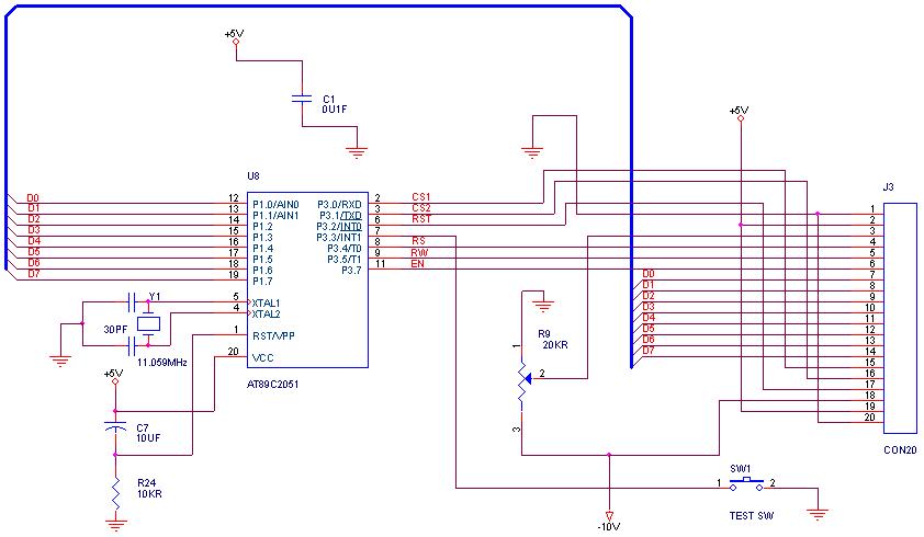
How can graphical LCDs be controlled using a microcontroller? Is there any datasheet available?
Graphical LCDs (Liquid Crystal Displays) are widely used in various electronic applications for displaying complex graphics and text. To control these displays with a microcontroller, several steps...

delay
This article outlines the construction of a simple microcontroller-based delay circuit designed for photographic applications, such as drop or high-speed photography. It is capable of controlling the trigger lag for cameras and flash units, generating periodic trigger pulses, or managing...

MICROCONTROLLER BASED AUTOMATIC ROOM LIGHT CONTROLLER
This project involves an automatic room light controller with a bidirectional visitor counter using a microcontroller. It is designed to manage room lighting and accurately count the number of individuals present. When a person enters the room, the counter increments...

Electronic TIC TAC TOE
This project is not to introduce Tic Tac Toe. Everyone knows this game. It is to introduce two features: bi-coloured LEDs, microcontrollers, and the skill of writing an ALGORITHM. You can use the project to learn the skills of creating...

Exploring Microcontrollers
Many of today's appliances feature displays and buttons. Instead of relying on motors and gears, numerous household items now incorporate embedded microcontrollers. This exploration focuses on how to experiment with microcontrollers at home.
Microcontrollers serve as the central processing units for...

GSM Remote Control 2 IN and 2 OUT Part 2 Schematic
The control of the system is managed by a Microchip PIC18F46K20-I/PT microcontroller, which is programmed with firmware to oversee the activity of the GSM/GPRS module, monitor the logic conditions of two opto-isolated inputs, and send commands to two relays within...

Crazy Looper Schematic
Two schematics are provided, one depicting the circuit without a programming port and the other including a programming port.
The first schematic represents a basic electronic circuit configuration that operates independently of a programming interface. This design may be suitable for...

Atmel AVR Microcontroller projects
A tiny speedometer/trip computer was constructed using an Atmel ATTiny2313 microcontroller and an HD44780-compatible character LCD display, along with a reed switch and magnets. This device measured the speed of a soapbox derby cart by attaching a permanent magnet to...