


AD524 differential shielded drive
#AD524
#differential amplifier
#shielded drive
#feedback circuit
#gain setting
#instrumentation amplifier
#signal conditioning
#precision amplifier

Description: The AD524 differential shielded drive is depicted in Fig. AD524. The RC1 and RC2 serve not only as gain setting components but also as part of the output feedback circuit, which includes an internal resistance of 20 kΩ. This operational amplifier is connected to the terminals A1 and A2, where the amplified output signal is directly applied to the input signal line shield. This configuration forms a differential input signal masking circuit that effectively shields against external interference signals and minimizes signal attenuation. This feature is particularly crucial for long-distance signal transmission.
The AD524 differential shielded drive employs a sophisticated design that incorporates operational amplifiers to achieve high fidelity in signal processing. The use of RC1 and RC2 for gain setting allows for precise control over the amplification level, ensuring optimal performance across various applications. The internal 20 kΩ resistance plays a critical role in establishing feedback, which stabilizes the amplifier's response and enhances linearity.
In this schematic, the connection of the operational amplifier to the terminals A1 and A2 is fundamental. The amplified output signal is routed through a shielded line, which serves to protect the signal from electromagnetic interference (EMI) and radio frequency interference (RFI). This shielding is essential in environments where external noise can significantly degrade the quality of the signal, such as in industrial settings or during long cable runs.
The differential input signal masking circuit is a key feature that distinguishes the AD524 design. By utilizing a differential input configuration, the circuit can reject common-mode signals, which are often the result of interference. This capability is vital for maintaining signal integrity, particularly in applications involving long-distance transmission, where attenuation and noise can severely impact performance.
Overall, the AD524 differential shielded drive is engineered to deliver reliable, high-quality signal amplification while minimizing the effects of external disturbances. Its design is particularly advantageous for applications requiring robust performance in challenging environments, ensuring that the integrity of the transmitted signal is preserved.AD524 differential shielded drive as shown in Fig. AD524 The RC:, RCz not only gain setting foot, also output feedback (internal 20kfl resistance) circuit part of this operatio nal amplifier is connected to the feet Al, A2, amplified output signal is directly applied to the input signal line shield It constitutes a differential input signal masking circuit, which can effectively shield external interference signals and reduce signal attenuation decreases. Especially for long-term transmission signal is particularly important.
The AD524 differential shielded drive employs a sophisticated design that incorporates operational amplifiers to achieve high fidelity in signal processing. The use of RC1 and RC2 for gain setting allows for precise control over the amplification level, ensuring optimal performance across various applications. The internal 20 kΩ resistance plays a critical role in establishing feedback, which stabilizes the amplifier's response and enhances linearity.
In this schematic, the connection of the operational amplifier to the terminals A1 and A2 is fundamental. The amplified output signal is routed through a shielded line, which serves to protect the signal from electromagnetic interference (EMI) and radio frequency interference (RFI). This shielding is essential in environments where external noise can significantly degrade the quality of the signal, such as in industrial settings or during long cable runs.
The differential input signal masking circuit is a key feature that distinguishes the AD524 design. By utilizing a differential input configuration, the circuit can reject common-mode signals, which are often the result of interference. This capability is vital for maintaining signal integrity, particularly in applications involving long-distance transmission, where attenuation and noise can severely impact performance.
Overall, the AD524 differential shielded drive is engineered to deliver reliable, high-quality signal amplification while minimizing the effects of external disturbances. Its design is particularly advantageous for applications requiring robust performance in challenging environments, ensuring that the integrity of the transmitted signal is preserved.AD524 differential shielded drive as shown in Fig. AD524 The RC:, RCz not only gain setting foot, also output feedback (internal 20kfl resistance) circuit part of this operatio nal amplifier is connected to the feet Al, A2, amplified output signal is directly applied to the input signal line shield It constitutes a differential input signal masking circuit, which can effectively shield external interference signals and reduce signal attenuation decreases. Especially for long-term transmission signal is particularly important.

A709 a simple differential amplifier circuit diagram
The simple differential amplifier circuit consists of two input signals, Vi1 and Vi2, which are connected through resistors R1, R3, and R4, forming a voltage divider circuit at the op-amp input. Vi1 is applied to the inverting input of the...

Differential amplifier circuit four connection methods and compare the characteristics of a
A differential amplifier circuit can be configured in four different connection methods, allowing for a comparison of characteristics such as gain and common-mode rejection ratio (CMRR). This analysis focuses on symmetrical circuits and their performance in handling common-mode signals.
The differential...

The instrumentation amplifier
It is advantageous to adjust the gain of an amplifier circuit without modifying more than one resistor value, unlike the previous design of the differential amplifier. The instrumentation amplifier builds upon the last version of the differential amplifier to provide...

Instrumentation-amplifier
LTC1043 and LT1013 dual operational amplifiers are utilized to construct a dual instrumentation amplifier with only two packages. A single double-pole double-throw (DPDT) switch converts the differential input into a ground-referenced single-ended signal at the input of the LT1013. When...
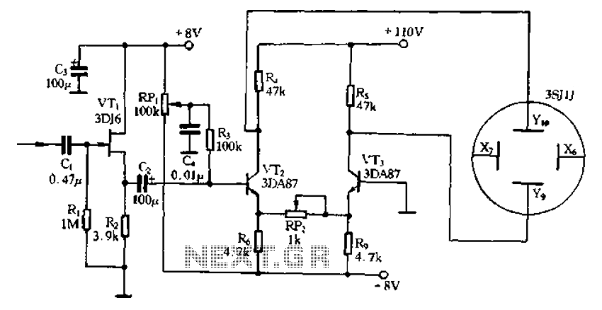
Application of the differential amplifier circuit in a simple small oscilloscope
Application of the differential amplifier circuit in a simple small oscilloscope.
The differential amplifier circuit is a crucial component in the design of a simple small oscilloscope. This circuit is designed to amplify the difference between two input voltage signals while...

Digital Controlled Precision Amplifier Circuit PCB
This circuit is a precision amplifier with digital control, designed for signal conditioning of low-output transducers operating in the millivolt range. The resistors R3 to R6 can be user-selected, with values ranging from 1 kilo-ohm to 1 mega-ohm, allowing for...

Having a differential amplifier and overcurrent protection for power supply circuit 2
The circuit features a current protection mechanism utilizing transistors VTa, VT4, and a sense resistor Ro. When an overcurrent or short-circuit fault occurs, the power supply cannot resume normal operation because the conduction condition of VT3 remains unchanged, resulting in...
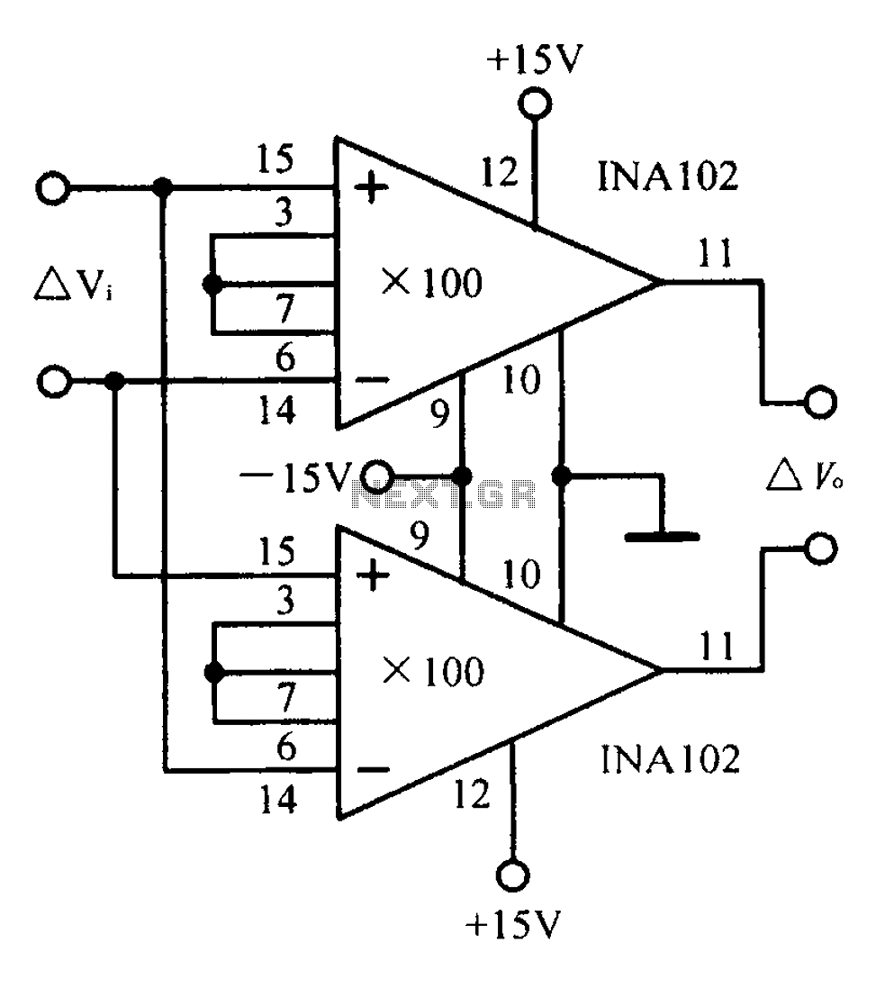
A differential input differential output amplifying circuit diagram
A differential input differential output amplifying circuit diagram.
A differential input differential output (DIDO) amplifier is a type of operational amplifier configuration that is designed to amplify the difference between two input signals while rejecting any signals that are common to...

Differential amplifier circuit
The differential amplifier is known for its stability and zero drift suppression. The circuit, as illustrated, utilizes two identical transistors, VT1 and VT2 (both 3DG6). The reference values for the component parameters are depicted in the figure. The circuit operates...