


cut the feed forward in the miller compensation with voltage buffer
#operational amplifier
#Miller compensation
#voltage buffer
#MOS technology
#enhancement mode
#input stage
#process parameters
#Al-gate
#n-channel

Description: An internally compensated operational amplifier has been fabricated using n-channel Al-gate MOS technology, utilizing only enhancement mode devices. The circuit is designed to ensure that its performance remains insensitive to process parameters. The input stage consists of a source-coupled differential amplifier, which produces a differential output signal that is sent to a differential-to-single-ended converter. This converter generates a single-ended version of the signal, which then drives a cascode stage. Feedback is applied around this stage through a source follower and a capacitor to implement a Miller compensation scheme. Another source follower, fed from the cascode stage, drives the output stage. The interdependence of the bias points among the stages ensures that their quiescent voltages track each other, maintaining stability across all stages except the final two. Frequency compensation is achieved through the capacitance C, which is Miller multiplied by the cascode stage, creating a dominant pole in conjunction with the output resistance of the differential-to-single-ended converter. The compensation capacitor C is not directly connected between the input and output of the cascode stage to avoid introducing a right half-plane zero, which degrades the amplifier's phase response at high frequencies. The right-half plane zero arises from feed-forward through the compensation capacitor, which can hinder frequency compensation. To mitigate this, a buffer implemented as a source follower is placed in series with C, preventing feed-forward and eliminating the right-half plane zero while allowing feedback that results in the desired dominant pole. The complete amplifier schematic is illustrated in the accompanying figure.
The operational amplifier described is a sophisticated circuit designed for high performance and stability, utilizing advanced MOS technology. The n-channel Al-gate MOS fabrication process allows for enhanced performance characteristics, particularly in terms of speed and power efficiency. The source-coupled differential amplifier at the input stage is crucial for achieving high common-mode rejection and low noise, which are essential for precision applications.
The differential-to-single-ended converter plays a vital role in transforming the differential output into a single-ended signal suitable for further processing. This conversion is critical in applications where a single-ended output is required, such as in many analog signal processing tasks. The cascode stage enhances the amplifier's output impedance, improving the overall gain and bandwidth of the amplifier.
The implementation of a Miller compensation scheme is a key aspect of maintaining stability across the operational amplifier's frequency response. By using a capacitor to create a dominant pole, the circuit can effectively manage gain and phase characteristics, ensuring that the amplifier remains stable under varying load conditions. The careful design choice to avoid direct connection of the compensation capacitor between the input and output of the cascode stage is a strategic decision to prevent the introduction of undesirable phase shifts that could compromise the amplifier's performance.
The addition of a source follower as a buffer in series with the compensation capacitor is an innovative solution to eliminate the right-half plane zero. This design choice not only maintains the integrity of the feedback loop but also enhances the overall frequency response of the amplifier, allowing it to perform optimally across a wide range of frequencies.
Overall, the operational amplifier's design reflects a thorough understanding of electronic circuit principles, ensuring that it can deliver high performance in demanding applications while maintaining robustness against variations in manufacturing processes. The schematic, as illustrated, provides a clear representation of the operational amplifier's architecture, highlighting the interconnections and functional blocks that contribute to its performance.An internally compensated operational amplifier is described which has been fabricated using n-channel Al-gate MOS technology. Only enhancement mode devices are used, and the circuit has been designed so that its performance is insensitive to process parameters.
A block diagram of the operational amplifier is shown in Fig. 1. The input stage is a source-coupled differential amplifier. The differential output signal of this stage is applied to a differential-to-single-ended converter, which develops a single-ended version of that signal. The converter drives a cascode stage, around which feedback is applied through a source follower and a capacitor, to implement a Miller compensation scheme.
Another source follower, fed from the cascode stage, drives the output stage. The bias point interdependence of the stages is such that their quiescent voltages track one another, so that all stages except the last two remain Frequency compensation of the circuit is accomplished through the capacitance C, shown in Fig. 1, which is Miller multiplied by the cascode stage and used to create a dominant pole in conjunction with the output resistance of the differential-to-single-ended converter.
The compensation capacitor C is not connected directly between the input and output of the cascode stage because for an inverting gain stage with simple pole splitting compensation, the compensation capacitor, in addition to introducing a dominant pole, also introduces a right half plane zero corresponding to ‰z = gm/C, where gm is the transconductance of the stage and C the compensation capacitance. The right-half plane zero is clearly undesirable, since it degrades the phase of the complete amplifier by 90 ° at high frequencies, while at the same time eliminating the effect of the dominant pole on the gain magnitude frequency response by stopping the 20 dB/decade rolloff created by it.
For the values of C required and for the values of gm that can be achieved, the frequency of the zero is lower than that of the crossover frequency and thus frequency compensation becomes impossible. Physically, the zero is caused by feed-forward through the compensation capacitor. To eliminate this feed forward, a buffer implemented by a source follower is placed in series with C, thus preventing the feedforward and therefore eliminating the right-half plane zero, while at the same time allowing feedback which gives rise to the desirable dominant pole.
The complete amplifier schematic is shown in the figure below.
The operational amplifier described is a sophisticated circuit designed for high performance and stability, utilizing advanced MOS technology. The n-channel Al-gate MOS fabrication process allows for enhanced performance characteristics, particularly in terms of speed and power efficiency. The source-coupled differential amplifier at the input stage is crucial for achieving high common-mode rejection and low noise, which are essential for precision applications.
The differential-to-single-ended converter plays a vital role in transforming the differential output into a single-ended signal suitable for further processing. This conversion is critical in applications where a single-ended output is required, such as in many analog signal processing tasks. The cascode stage enhances the amplifier's output impedance, improving the overall gain and bandwidth of the amplifier.
The implementation of a Miller compensation scheme is a key aspect of maintaining stability across the operational amplifier's frequency response. By using a capacitor to create a dominant pole, the circuit can effectively manage gain and phase characteristics, ensuring that the amplifier remains stable under varying load conditions. The careful design choice to avoid direct connection of the compensation capacitor between the input and output of the cascode stage is a strategic decision to prevent the introduction of undesirable phase shifts that could compromise the amplifier's performance.
The addition of a source follower as a buffer in series with the compensation capacitor is an innovative solution to eliminate the right-half plane zero. This design choice not only maintains the integrity of the feedback loop but also enhances the overall frequency response of the amplifier, allowing it to perform optimally across a wide range of frequencies.
Overall, the operational amplifier's design reflects a thorough understanding of electronic circuit principles, ensuring that it can deliver high performance in demanding applications while maintaining robustness against variations in manufacturing processes. The schematic, as illustrated, provides a clear representation of the operational amplifier's architecture, highlighting the interconnections and functional blocks that contribute to its performance.An internally compensated operational amplifier is described which has been fabricated using n-channel Al-gate MOS technology. Only enhancement mode devices are used, and the circuit has been designed so that its performance is insensitive to process parameters.
A block diagram of the operational amplifier is shown in Fig. 1. The input stage is a source-coupled differential amplifier. The differential output signal of this stage is applied to a differential-to-single-ended converter, which develops a single-ended version of that signal. The converter drives a cascode stage, around which feedback is applied through a source follower and a capacitor, to implement a Miller compensation scheme.
Another source follower, fed from the cascode stage, drives the output stage. The bias point interdependence of the stages is such that their quiescent voltages track one another, so that all stages except the last two remain Frequency compensation of the circuit is accomplished through the capacitance C, shown in Fig. 1, which is Miller multiplied by the cascode stage and used to create a dominant pole in conjunction with the output resistance of the differential-to-single-ended converter.
The compensation capacitor C is not connected directly between the input and output of the cascode stage because for an inverting gain stage with simple pole splitting compensation, the compensation capacitor, in addition to introducing a dominant pole, also introduces a right half plane zero corresponding to ‰z = gm/C, where gm is the transconductance of the stage and C the compensation capacitance. The right-half plane zero is clearly undesirable, since it degrades the phase of the complete amplifier by 90 ° at high frequencies, while at the same time eliminating the effect of the dominant pole on the gain magnitude frequency response by stopping the 20 dB/decade rolloff created by it.
For the values of C required and for the values of gm that can be achieved, the frequency of the zero is lower than that of the crossover frequency and thus frequency compensation becomes impossible. Physically, the zero is caused by feed-forward through the compensation capacitor. To eliminate this feed forward, a buffer implemented by a source follower is placed in series with C, thus preventing the feedforward and therefore eliminating the right-half plane zero, while at the same time allowing feedback which gives rise to the desirable dominant pole.
The complete amplifier schematic is shown in the figure below.

A delay circuit using an operational amplifier
A delay circuit utilizing an operational amplifier functions as a comparator, providing high timing accuracy. The timer's delay range is from 1 to 30 seconds. The delay time is determined by resistors Ri, RP, and capacitor C. By adjusting RP,...

GF2A op amp audio amplifier circuit diagram
The operational amplifier A is utilized in an audio preamplifier circuit. Its advantages include compact size, low noise, low power consumption, and excellent consistency. The operational amplifier can achieve significant negative feedback while increasing output without distortion. The signal distortion...

Cosine wave Oscillator
This circuit is designed to output both a sine wave and a cosine wave. The design utilizes an operational amplifier, with the output frequency determined by component values set to 1Hz. The first operational amplifier generates a 1Hz sine wave,...

lowvoltage ac voltmeter
The primary component of this circuit is an operational amplifier (such as the 741 or 351), configured as an amplifier with a feedback circuit that consists of a diode bridge full-wave rectifier. An ammeter is connected to the rectifier circuit,...

ZKJ-S-type buffer controller circuit
The ZKJ-S-type buffer controller circuit is designed for motor starting slip control. This buffer controller is composed of two operational amplifiers, Ai and Az. The operational amplifier Ai functions as a speed amplifier that saturates, while Az acts as an...

Delay circuit of a multi-level output
A multi-stage delay circuit is presented in this schematic. The operational amplifiers are configured as comparators. Operational amplifier A1 operates when the voltage at the inverting input exceeds + VE. As the voltage at the inverting input of operational amplifiers...

Precision current sink sourcel
An operational amplifier circuit can provide a constant voltage source with a high amplification factor and substantial load current. Even with significant variations in circuit parameters, the output voltage maintains high precision. The output current limit is managed by transistors...

Operational-amplifiers
This is a single gain-of-100 amplifier with a gain-bandwidth product of 20 MHz. The primary limitation in performance is the low slew rate of 0.3 V/μs imposed by the charging of Ccomp. The effects of slew rate and compensation are...
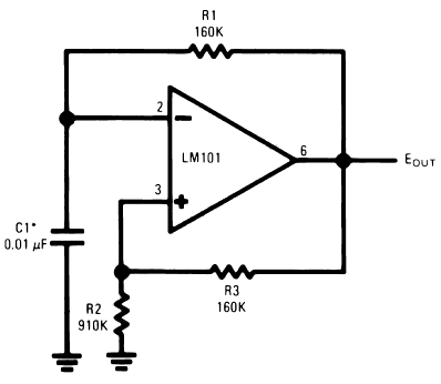
operational amplifier op amp oscillator
The timing capacitor (C1) generates multiple time constants, facilitating substantial voltage fluctuations at the input, attributable to the LM101's extensive input voltage range. It is advisable to decrease the value of resistor R2 and to increase the capacitance of C1...