


Improved differential circuit diagram

Description: The modification of the differential circuit is illustrated. In Figure A1, an integrator is depicted, and the output is presented.
The circuit modification involves integrating the differential circuit with an integrator component, which plays a crucial role in signal processing applications. The integrator is designed to output a voltage that is proportional to the integral of the input signal over time. This is particularly useful in applications where the cumulative effect of a signal is required, such as in analog computing or control systems.
In Figure A1, the integrator is typically implemented using an operational amplifier (op-amp) configured in an inverting mode. The input signal is applied to the inverting terminal of the op-amp through a resistor, while a capacitor is connected between the output and the inverting terminal, forming a feedback loop. The non-inverting terminal is grounded.
The output voltage of the integrator can be expressed mathematically as V_out(t) = -(1/RC) ∫ V_in(t) dt, where R is the resistance, C is the capacitance, and V_in(t) is the input voltage. This equation indicates that the output voltage is the negative integral of the input voltage, scaled by the time constant RC of the circuit.
Additionally, it is essential to consider the frequency response of the integrator, as it can significantly influence the performance of the overall differential circuit. The integrator will have a high gain at low frequencies and will attenuate high-frequency signals, which can lead to phase shifts and potential instability in certain applications. Therefore, proper selection of the resistor and capacitor values is critical to ensure that the integrator operates effectively within the desired frequency range.
Overall, the integration of the differential circuit with an integrator enhances its functionality, enabling it to process signals that require accumulation over time, thereby expanding the potential applications in various electronic systems. As shown for the modification of the differential circuit. Figure, A1 is an integrator, the output is
The circuit modification involves integrating the differential circuit with an integrator component, which plays a crucial role in signal processing applications. The integrator is designed to output a voltage that is proportional to the integral of the input signal over time. This is particularly useful in applications where the cumulative effect of a signal is required, such as in analog computing or control systems.
In Figure A1, the integrator is typically implemented using an operational amplifier (op-amp) configured in an inverting mode. The input signal is applied to the inverting terminal of the op-amp through a resistor, while a capacitor is connected between the output and the inverting terminal, forming a feedback loop. The non-inverting terminal is grounded.
The output voltage of the integrator can be expressed mathematically as V_out(t) = -(1/RC) ∫ V_in(t) dt, where R is the resistance, C is the capacitance, and V_in(t) is the input voltage. This equation indicates that the output voltage is the negative integral of the input voltage, scaled by the time constant RC of the circuit.
Additionally, it is essential to consider the frequency response of the integrator, as it can significantly influence the performance of the overall differential circuit. The integrator will have a high gain at low frequencies and will attenuate high-frequency signals, which can lead to phase shifts and potential instability in certain applications. Therefore, proper selection of the resistor and capacitor values is critical to ensure that the integrator operates effectively within the desired frequency range.
Overall, the integration of the differential circuit with an integrator enhances its functionality, enabling it to process signals that require accumulation over time, thereby expanding the potential applications in various electronic systems. As shown for the modification of the differential circuit. Figure, A1 is an integrator, the output is

Homemade whole integrated circuit amplifiers 01
The circuit depicted in Figure 5-60 and Figure 6 utilizes an operational amplifier (op-amp) configured as a channel pre-amplifier to address the signal loss introduced by the tone control circuit. Additionally, another group of op-amps forms a channel-driven stage amplifier...

Precision current sink sourcel
An operational amplifier circuit can provide a constant voltage source with a high amplification factor and substantial load current. Even with significant variations in circuit parameters, the output voltage maintains high precision. The output current limit is managed by transistors...
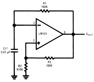
operational amplifier op amp oscillator
The timing capacitor (C1) generates multiple time constants, facilitating substantial voltage fluctuations at the input, attributable to the LM101's extensive input voltage range. It is advisable to decrease the value of resistor R2 and to increase the capacitance of C1...

Field-programmable Operational Transresistance Amplifier using Floating-gate MOSFETs
A comprehensive design procedure is proposed for the development of Field-programmable/Reconfigurable Analog Integrated CMOS circuits. Instead of relying on iterative simulation steps to meet design specifications by adjusting the W/L ratios of the FETs, first-order classroom equations are utilized to...
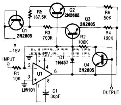
Nonlinear Operational Amplifier Circuit
This operational amplifier circuit utilizes resistor and transistor feedback elements to function as a nonlinear amplifier. The resistors R4 and R6 can be adjusted to modify the breakpoints as needed.
This operational amplifier circuit is designed to operate within the nonlinear...

ZKJ-S-type buffer controller circuit
The ZKJ-S-type buffer controller circuit is designed for motor starting slip control. This buffer controller is composed of two operational amplifiers, Ai and Az. The operational amplifier Ai functions as a speed amplifier that saturates, while Az acts as an...

X100 operational amplifier
The amplifier has a gain-bandwidth product of 20 MHz, with a slew rate of 0.3 V/µs.
The amplifier's gain-bandwidth product (GBP) of 20 MHz indicates that the product of the amplifier's gain and the bandwidth at which that gain is applicable...

Cosine wave Oscillator
This circuit is designed to output both a sine wave and a cosine wave. The design utilizes an operational amplifier, with the output frequency determined by component values set to 1Hz. The first operational amplifier generates a 1Hz sine wave,...

9400 Selling Leads 9400 Datasheet PDF
The absolute-value integrator circuit generates the effect of producing negative frequencies when the input signal is negative. It accomplishes this by allowing the counter to count up for positive voltage and count down for negative voltage. The specific types of...