


Low-input-capacitance-buffer

Description: Q1 and Q2 form a simple, high-speed FET input buffer. Q1 operates as a source follower, while Q2 serves as a current-source load that regulates the drain-source channel current. The LT1010 buffer is utilized to provide output drive capability for cables or any required load. The LTC1052 stabilizes the circuit by comparing the filtered output of the circuit to a similarly filtered version of the input signal. The amplified difference between these signals is employed to adjust the bias of Q2, thereby influencing the channel current of Q1. This adjustment forces Q1's output voltage to align with the necessary voltage to match the circuit's input and output potentials. A diode in Q1's source line prevents forward biasing of the gate, and a 2000-pF capacitor at A1 ensures stable loop compensation. The RC network at A1's output prevents it from experiencing high-speed edges coupled through Q2's collector-base junction. Additionally, A2's output is fed back to the shield surrounding Q1's gate lead, effectively bootstrapping the circuit's input capacitance to below 1 pF.
The circuit operates as a high-speed buffer, utilizing FET technology to achieve low input capacitance and high output drive capability. Q1, as the source follower, provides a high input impedance and low output impedance, making it ideal for interfacing with various loads without significant signal degradation. The role of Q2 as a current source is critical; it maintains a constant current through Q1, thus ensuring linearity and stability across different operating conditions.
The LT1010 buffer is designed to handle significant output loads, making it suitable for driving long cables or low-impedance loads without distortion. The LTC1052 adds a layer of stability by continuously comparing the output signal with the input, allowing for real-time adjustments to Q2's bias. This feedback mechanism is essential for maintaining signal integrity, particularly in high-speed applications where variations in load can lead to significant performance variations.
The inclusion of the diode in Q1's source line is a protective measure to prevent the gate from becoming forward biased, which could lead to unwanted conduction paths and affect the performance of the buffer. The 2000-pF capacitor at A1 plays a crucial role in stabilizing the feedback loop, ensuring that the circuit can respond quickly to changes in input without oscillation or instability.
The RC network at A1's output is strategically placed to filter out high-frequency noise and prevent signal distortion from fast transients that may couple through Q2's collector-base junction. This design consideration enhances the overall performance of the buffer, ensuring that it can handle high-speed signals effectively.
Furthermore, the feedback from A2 to the shield around Q1's gate lead is an innovative approach to reduce the effective input capacitance of the circuit. By bootstrapping the input capacitance to below 1 pF, the circuit achieves exceptionally high bandwidth and fast response times, making it suitable for advanced applications in high-frequency electronics. Overall, this circuit design exemplifies the integration of various components to achieve a robust, high-performance buffer suitable for demanding electronic applications.Ql and Q2 constitute a simple, high-speed FET input buffer.·Ql functions as a source follower, with the Q2 current-source load setting the drain-source channel current. The LT1010 buffer provides output drive capability for cables or whatever load is required. The LTC1052 stabilizes the circuit by comparing the filtered circuit output to a similarly filtered version of the input signal.
The amplified difference between these signals is used to set Q2"s bias, and hence Ql"s channel current. This forces Ql"s V0 s to whatever voltage is required to match the circuit"s input and output potentials. The diode in Ql"s source line ensures that the gate never forward biases and the 2000-pF capacitor at Al provides stable loop compensation.
The rc network in Al "s output prevents it from seeing high-speed edges coupled through Q2"s collector-base ]unction. A2"s output is also fed back to the shield around Ql "s gate lead, bootstrapping the circuit"s effective input capacitance to less than 1 pF.
The circuit operates as a high-speed buffer, utilizing FET technology to achieve low input capacitance and high output drive capability. Q1, as the source follower, provides a high input impedance and low output impedance, making it ideal for interfacing with various loads without significant signal degradation. The role of Q2 as a current source is critical; it maintains a constant current through Q1, thus ensuring linearity and stability across different operating conditions.
The LT1010 buffer is designed to handle significant output loads, making it suitable for driving long cables or low-impedance loads without distortion. The LTC1052 adds a layer of stability by continuously comparing the output signal with the input, allowing for real-time adjustments to Q2's bias. This feedback mechanism is essential for maintaining signal integrity, particularly in high-speed applications where variations in load can lead to significant performance variations.
The inclusion of the diode in Q1's source line is a protective measure to prevent the gate from becoming forward biased, which could lead to unwanted conduction paths and affect the performance of the buffer. The 2000-pF capacitor at A1 plays a crucial role in stabilizing the feedback loop, ensuring that the circuit can respond quickly to changes in input without oscillation or instability.
The RC network at A1's output is strategically placed to filter out high-frequency noise and prevent signal distortion from fast transients that may couple through Q2's collector-base junction. This design consideration enhances the overall performance of the buffer, ensuring that it can handle high-speed signals effectively.
Furthermore, the feedback from A2 to the shield around Q1's gate lead is an innovative approach to reduce the effective input capacitance of the circuit. By bootstrapping the input capacitance to below 1 pF, the circuit achieves exceptionally high bandwidth and fast response times, making it suitable for advanced applications in high-frequency electronics. Overall, this circuit design exemplifies the integration of various components to achieve a robust, high-performance buffer suitable for demanding electronic applications.Ql and Q2 constitute a simple, high-speed FET input buffer.·Ql functions as a source follower, with the Q2 current-source load setting the drain-source channel current. The LT1010 buffer provides output drive capability for cables or whatever load is required. The LTC1052 stabilizes the circuit by comparing the filtered circuit output to a similarly filtered version of the input signal.
The amplified difference between these signals is used to set Q2"s bias, and hence Ql"s channel current. This forces Ql"s V0 s to whatever voltage is required to match the circuit"s input and output potentials. The diode in Ql"s source line ensures that the gate never forward biases and the 2000-pF capacitor at Al provides stable loop compensation.
The rc network in Al "s output prevents it from seeing high-speed edges coupled through Q2"s collector-base ]unction. A2"s output is also fed back to the shield around Ql "s gate lead, bootstrapping the circuit"s effective input capacitance to less than 1 pF.

FET Preamplifier Circuit
A Field Effect Transistor (FET) is an amplifying device where the output current is influenced by the input voltage. The FET preamplifier described here is sensitive.
The Field Effect Transistor (FET) operates by utilizing an electric field to control the flow...

MPF102 FET Preamplifier Arduino
A Darlington transistor can enhance circuit performance, although it introduces slight complexity. The advantage of using a Darlington configuration lies in its capability to achieve low output impedance. The recommended component is the 2N6426 from Mouser, with alternatives such as...
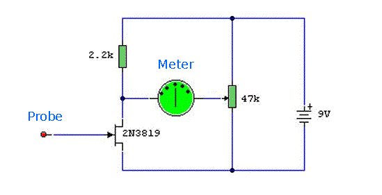
static detector negative ion detector
A sensitive detector for static electricity is based on a single Field Effect Transistor (FET). It can also be utilized to detect the presence of negative ions or to test a negative ion generator. This circuit takes advantage of the...

High Impedance Low Capacitance Buffer/Amplifier
These are circuits of high impedance low capacitance buffer and high impedance low capacitance amplifier. The first figure is a high impedance low capacitance.
High impedance low capacitance circuits are critical in various electronic applications, particularly in signal processing and sensor...

Group items tagged circuit Robotics
The 1-megohm resistor protects the FET from potential damage caused by accidental sparks to its gate lead. The circuit functions adequately without this resistor; however, it is advised not to intentionally apply a charge to the gate wire using a...

FET VOLTMETER 1
This FET voltmeter (FETVM) serves as a replacement for the vacuum tube voltmeter (VTVM) and eliminates the need for a standard line cord. Additionally, the drift rates of field-effect transistors (FETs) are significantly better than those of vacuum tube circuits,...
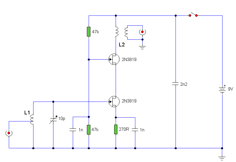
Band 2 Preamplifier
The circuit utilizes two 2N3819 FETs arranged in a cascode configuration. The lower FET functions in common source mode, while the upper FET operates in common gate mode, achieving full high-frequency gain. The lower FET is adjustable, enabling tuning to...

Band 2 Preamplifier
The circuit utilizes two 2N3819 FETs arranged in a cascode configuration. The lower FET functions in common source mode, while the upper FET operates in common gate mode, achieving full high-frequency gain. The lower FET is tunable, enabling peak tuning...

Static Electricity Detector
This circuit relies upon the extra high input impedance of a FET, and also demonstrates the gate terminals sensitivity to changes in voltage. The gate terminal here is left open circuit, connected only to the "probe" this being just a...