


Multiplicative -DA converter electronic attenuator
#DA converter
#analog switch
#attenuator
#8-bit
#multiplicative
#AD7s23
#voltage output
#digital input
#analog input

Description: The AD7s23 is an 8-bit multiplying digital-to-analog (DA) converter that generates an output voltage based on both the analog and digital inputs. The unit comprises eight analog switches and utilizes a ladder network configuration. This ladder serves as a damping circuit. Due to the current output from the ladder network, a current-to-voltage conversion amplifier, such as the OP12c, is required. The ladder network typically has a resistance of approximately 10kΩ, which may vary within a range of 5kΩ to 20kΩ without inducing significant errors, provided that the relative values of each resistor in the ladder network are consistent. The components are integrated on a single chip, allowing for a uniform temperature coefficient, making it suitable for variable attenuation applications. To achieve accurate attenuation, a coarse adjustment is necessary. If the input resistance is low, typically around 20kΩ, a buffer amplifier can be added at the input stage.
The AD7s23 architecture is designed to efficiently convert digital signals into corresponding analog voltages with high precision. The eight analog switches are pivotal in controlling the flow of current through the ladder network, which is configured to provide a linear response across its range. The ladder network's design is crucial for maintaining the integrity of the output signal, as it dictates how the digital inputs are translated into analog voltages.
The current-to-voltage conversion amplifier, such as the OP12c, plays a vital role in transforming the current output from the ladder into a usable voltage level. This conversion is essential for interfacing with other analog components or systems that require voltage signals. The choice of approximately 10kΩ for the ladder network's resistance is a balance between minimizing power consumption and ensuring adequate signal integrity. The tolerance of the resistors in this network is critical; mismatched resistor values can lead to non-linearities and inaccuracies in the output voltage.
The integration of components on a single chip not only enhances performance through reduced parasitic elements but also ensures that the temperature characteristics of the components are closely matched. This matching is particularly important in applications where temperature variations can affect performance, leading to drift in the output signal.
In scenarios where input resistance is a concern, such as when interfacing with high-impedance sources, the inclusion of a buffer amplifier at the input stage helps isolate the ladder network from the source. This isolation prevents loading effects that could distort the input signal, thus preserving the fidelity of the conversion process. The design of the AD7s23 makes it a robust solution for applications requiring precise analog outputs from digital signals, such as in signal processing, control systems, and instrumentation.AD7s23 is an 8-bit multiplication DA converter, the output voltage of the analog input and the digital input of the product. Inside! Unit consists of eight analog switches (cha ngeover contact) and said. 2 Lu ladder network configuration, use the ladder as a damping circuit. Because the ladder network current output, so the need to use the current-voltage conversion amplifier OP12c by the ladder network of approximately iOkQ, there may not within the scope of s ~ 20kQ ~ cause, but as long as the relative value of each resistor ladder Dayton agreement is not It will cause errors. With elements on a chip, the temperature coefficient easily consistent, it is suitable as a variable attenuation is reduced.
In order to get the correct attenuation shall be carried out with the coarse ore roar. If the authentication is s ~ 20kcJ input resistance of small, can be added at the input end of the buffer amplifier.
The AD7s23 architecture is designed to efficiently convert digital signals into corresponding analog voltages with high precision. The eight analog switches are pivotal in controlling the flow of current through the ladder network, which is configured to provide a linear response across its range. The ladder network's design is crucial for maintaining the integrity of the output signal, as it dictates how the digital inputs are translated into analog voltages.
The current-to-voltage conversion amplifier, such as the OP12c, plays a vital role in transforming the current output from the ladder into a usable voltage level. This conversion is essential for interfacing with other analog components or systems that require voltage signals. The choice of approximately 10kΩ for the ladder network's resistance is a balance between minimizing power consumption and ensuring adequate signal integrity. The tolerance of the resistors in this network is critical; mismatched resistor values can lead to non-linearities and inaccuracies in the output voltage.
The integration of components on a single chip not only enhances performance through reduced parasitic elements but also ensures that the temperature characteristics of the components are closely matched. This matching is particularly important in applications where temperature variations can affect performance, leading to drift in the output signal.
In scenarios where input resistance is a concern, such as when interfacing with high-impedance sources, the inclusion of a buffer amplifier at the input stage helps isolate the ladder network from the source. This isolation prevents loading effects that could distort the input signal, thus preserving the fidelity of the conversion process. The design of the AD7s23 makes it a robust solution for applications requiring precise analog outputs from digital signals, such as in signal processing, control systems, and instrumentation.AD7s23 is an 8-bit multiplication DA converter, the output voltage of the analog input and the digital input of the product. Inside! Unit consists of eight analog switches (cha ngeover contact) and said. 2 Lu ladder network configuration, use the ladder as a damping circuit. Because the ladder network current output, so the need to use the current-voltage conversion amplifier OP12c by the ladder network of approximately iOkQ, there may not within the scope of s ~ 20kQ ~ cause, but as long as the relative value of each resistor ladder Dayton agreement is not It will cause errors. With elements on a chip, the temperature coefficient easily consistent, it is suitable as a variable attenuation is reduced.
In order to get the correct attenuation shall be carried out with the coarse ore roar. If the authentication is s ~ 20kcJ input resistance of small, can be added at the input end of the buffer amplifier.

High frequency analog switch
The commutator circuit delivers low impedance gate drive to the PN4091 analog switch for both on and off drive conditions. This circuit also achieves near-ideal gate drive conditions for high-frequency signal handling by offering low AC impedance during off drive...

MAX4685 circuit and input current limit resistors
A request for advice regarding the connection diagram of the MAX4685 analog switch is presented. The circuit involves two inputs, VI1 and VI2.
The MAX4685 is a low-voltage, dual analog switch designed for low on-resistance and high-speed switching applications. In a...

Analog Line Switch Circuit
This analog switch circuit is designed to switch an analog line on or off. It consists of two analog switches in integrated circuit (IC) form that are controlled by two pushbuttons.
The described analog switch circuit utilizes two integrated analog switches...

Adjustable Attenuator for Oscilloscope
The input attenuator uses a commutating capacitor to cancel the input capacitance of the FET buffer (see DC-10 MHz amp schematic). The commutating capacitors are absolutely necessary to cancel the effect of the input capacitance to the DC-10MHz amplifier. The...

Digitally-programmable-attenuator
The first stage is a simple buffer used to isolate the signal source from the following attenuator stages. Each subsequent stage is preceded by a voltage divider formed by two resistors and a CMOS switch. When the CMOS switch for...

differential analog switch circuit
This circuit is designed for differential analog circuit switches. The FM1208 monolithic dual differential multiplexer is utilized in applications where the RDS (ON) must be closely matched. The RDS (ON) for the monolithic dual multiplexer operates with a precision better...

DTL-TTL controlled buffered analog switch
This analog switch utilizes the 2N4860 JFET, which features a low on-resistance of 25 ohms and minimal leakage current. The LM102 is employed as a voltage buffer in the circuit. Additionally, this configuration can be modified for use in a...
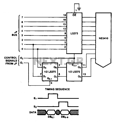
8-bit bus interface
The double latch technique ensures that valid data is latched to the Digital-to-Analog Converter (DAC) until it is updated by the E2 pulse. The timing of this process will depend on the specific processor utilized.
The double latch technique is a...

OSU8 Microprocessor Project (1994)
OSU8 began as a student project in 1994 to create a simple but functional 8-bit microprocessor, starting with a definition of the architecture to implementation in a Xilinx FPGA chip, and full-custom CMOS implementation. Over a period of about six...