


Noninverting gain circuit diagram by the MAX4107
#MAX4107
#noninverting amplifier
#ADC buffer
#gain circuit
#RF resistor
#RG resistor
#amplifier gain
#signal conditioning
#analog circuit
#buffer amplifier

Description: The inverting gain circuit utilizing the MAX4107 is configured as an ADC input buffer. The gain of the amplifier is established by the ratio of resistors RF and RG, which set the gain figure to approximately 10.
The inverting gain circuit using the MAX4107 operational amplifier is designed to function as an analog-to-digital converter (ADC) input buffer. The circuit configuration allows for the amplification of input signals while maintaining a high input impedance and low output impedance, which is crucial for interfacing with ADCs.
In this configuration, the gain of the amplifier is determined by the feedback resistor (RF) and the input resistor (RG). The relationship governing the gain (Av) of the inverting amplifier is given by the formula: Av = -RF/RG. For this particular design, the resistors are selected such that the gain is set to approximately 10. This means that for every 1V input signal, the output will be -10V, inverting the phase of the signal while amplifying its magnitude.
The choice of RF and RG values must be made carefully to ensure stability and linearity of the amplifier. Additionally, the MAX4107 is known for its low noise and high speed, making it suitable for high-frequency applications. Proper bypass capacitors should be placed close to the power supply pins of the MAX4107 to minimize power supply noise and ensure stable operation.
In summary, this inverting gain circuit effectively amplifies signals for ADC applications, providing a reliable interface with the necessary gain characteristics. As shown in FIG inverting gain circuit from the MAX4107 configured as ADC input buffers. Amplifier gain is determined by the ratio of RF and RG, resistors set the gain figure o f about 10.
The inverting gain circuit using the MAX4107 operational amplifier is designed to function as an analog-to-digital converter (ADC) input buffer. The circuit configuration allows for the amplification of input signals while maintaining a high input impedance and low output impedance, which is crucial for interfacing with ADCs.
In this configuration, the gain of the amplifier is determined by the feedback resistor (RF) and the input resistor (RG). The relationship governing the gain (Av) of the inverting amplifier is given by the formula: Av = -RF/RG. For this particular design, the resistors are selected such that the gain is set to approximately 10. This means that for every 1V input signal, the output will be -10V, inverting the phase of the signal while amplifying its magnitude.
The choice of RF and RG values must be made carefully to ensure stability and linearity of the amplifier. Additionally, the MAX4107 is known for its low noise and high speed, making it suitable for high-frequency applications. Proper bypass capacitors should be placed close to the power supply pins of the MAX4107 to minimize power supply noise and ensure stable operation.
In summary, this inverting gain circuit effectively amplifies signals for ADC applications, providing a reliable interface with the necessary gain characteristics. As shown in FIG inverting gain circuit from the MAX4107 configured as ADC input buffers. Amplifier gain is determined by the ratio of RF and RG, resistors set the gain figure o f about 10.

Low-distortion-video-buffer
This buffer amplifier's overall harmonic distortion is low at 0.01% or less at a 3-V RMS output into a 500-ohm load without overall feedback. The LT1010CT features a slew rate of 100 V/µs, a video bandwidth of 20 MHz, and...

Back radiation small buffer amplifier
A back radiation small buffer amplifier is presented, featuring an inverse radiation small buffer amplifier configuration. The circuit is composed of three transistors connected in series, functioning as a buffer amplifier. This design can be utilized in output amplifiers or...

Signal Conditioning Analog Front-end for Microcontrollers
The I/O board incorporates 16-bit resolution voltage analog inputs and outputs, along with a 4-20mA current loop transmitter and receiver for microcontroller applications. The document discusses amplifier circuits and schematics, including a signal conditioning variable gain amplifier, analog filter, and...

Signal Conditioners Information
Signal conditioning involves a series of operations applied to a signal to make it compatible for interfacing with other devices or systems. Signal conditioners are the devices that execute this operation, featuring both an input and an output. Typically, the...

28Db-noninverting-amplifier
The physical circuit layout is extremely critical. Breadboarding is not recommended. A double-sided copper-clad printed circuit board will result in more favorable system operation.
The design and implementation of electronic circuits require careful consideration of the physical layout, as it significantly...

ADT70 internal functional block diagram
The ADI I70 is a signal conditioning integrated circuit designed for RTD/PRTD applications, particularly suitable for 1K and 100Ω platinum RTDs (PRTDs). The ADT70 features an integrated instrumentation amplifier, an operational amplifier, a 2.5V reference power supply, and a matching...
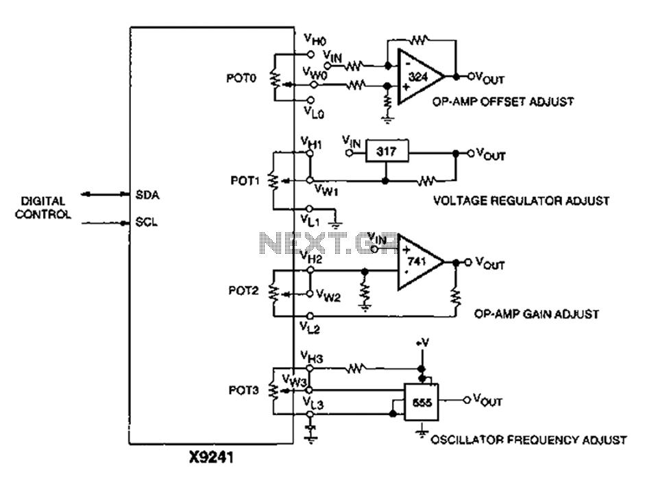
Corrector circuit diagram of an analog circuit
A XICOR X9241 POT IC module can be utilized to modify the four digital analog circuits, as depicted in the schematic.
The XICOR X9241 is a digital potentiometer integrated circuit designed for precise adjustment of analog signal levels in various electronic...

buffer amplifiers
This class of amplifier is designed to follow low-level stages, such as a crystal oscillator. An oscillator requires an intermediate stage to prevent loading, ensuring that the input impedance is sufficiently high to avoid significant loading on the oscillator. This...

Buffer amplifier
A buffer amplifier is utilized as a transistor emitter follower buffer amplifier for applications that necessitate a high input impedance. The circuit employs a complementary push-pull configuration. The signal input is connected to the base of transistor VT1, which features...