


Schmitt trigger
#schmitt trigger
#op-amp
#comparator
#hysteresis
#voltage threshold
#trigger points
#adjustable
#signal conditioning
#electronics
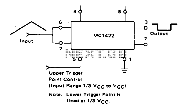
Description: The lower trigger point is fixed at a percentage of Vcc, while the upper trigger point can be adjusted using Pin 5, allowing it to vary from Vi to slightly less than Vcc. The Schmitt trigger is capable of operating with input frequencies of up to 50 kHz.
The described circuit employs a Schmitt trigger configuration that utilizes hysteresis to provide stable switching characteristics. The lower trigger point, fixed at a percentage of the supply voltage (Vcc), ensures that the output transitions to a low state when the input voltage falls below this threshold. This fixed lower threshold is essential for preventing noise from causing unintended switching.
The upper trigger point is adjustable through Pin 5, which allows for fine-tuning of the transition from low to high output. This adjustability is crucial in applications where precise control over the switching threshold is necessary. The ability to set the upper threshold slightly below Vcc provides flexibility in accommodating various input signal levels while ensuring reliable operation.
The Schmitt trigger's capability to handle input frequencies up to 50 kHz indicates its suitability for high-speed digital applications. This frequency range allows the circuit to effectively process rapid signal changes without distortion or delay, making it ideal for use in pulse-width modulation, signal conditioning, and other digital signal applications.
Overall, the combination of a fixed lower trigger point and an adjustable upper trigger point, along with the high-frequency operation, makes this Schmitt trigger circuit versatile for a wide range of electronic applications. The design ensures robust performance in environments where signal integrity and precise control are paramount.The lower trigger point is fixed at % Vcc, but the upper trigger point is adjustable by means of Pin 5 from Vi Vcc to slightly less than Vcc The Schmitt trigger will operate with input frequencies up to 50 kHz.
The described circuit employs a Schmitt trigger configuration that utilizes hysteresis to provide stable switching characteristics. The lower trigger point, fixed at a percentage of the supply voltage (Vcc), ensures that the output transitions to a low state when the input voltage falls below this threshold. This fixed lower threshold is essential for preventing noise from causing unintended switching.
The upper trigger point is adjustable through Pin 5, which allows for fine-tuning of the transition from low to high output. This adjustability is crucial in applications where precise control over the switching threshold is necessary. The ability to set the upper threshold slightly below Vcc provides flexibility in accommodating various input signal levels while ensuring reliable operation.
The Schmitt trigger's capability to handle input frequencies up to 50 kHz indicates its suitability for high-speed digital applications. This frequency range allows the circuit to effectively process rapid signal changes without distortion or delay, making it ideal for use in pulse-width modulation, signal conditioning, and other digital signal applications.
Overall, the combination of a fixed lower trigger point and an adjustable upper trigger point, along with the high-frequency operation, makes this Schmitt trigger circuit versatile for a wide range of electronic applications. The design ensures robust performance in environments where signal integrity and precise control are paramount.The lower trigger point is fixed at % Vcc, but the upper trigger point is adjustable by means of Pin 5 from Vi Vcc to slightly less than Vcc The Schmitt trigger will operate with input frequencies up to 50 kHz.

Suitable comparator circuit headset detection
A headphone type detection circuit is illustrated in the attached figure. The 2.2k RMIC-BIAS resistor connected to the audio controller provides a low-noise reference voltage (VMIC-REF). When the audio jack is inserted, the VMIC-REF voltage through RMIC-BIAS is applied to...

Schmitt Trigger VU Meter
The schematic indicates that the input is routed through a voltage divider. This configuration is essential for the operation of the Schmitt triggers, which all activate under certain conditions.
The voltage divider in the schematic serves to scale down the input...
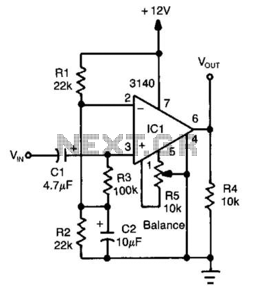
Sine-Wave/Square-Wave Converter
An operational amplifier (op amp) configured as a comparator generates a 10-V peak-to-peak square wave output with a 100-mV input signal, operating up to 15 kHz. Adjust resistor R5 to achieve symmetry in the square wave at low input levels.
The...

Op-Amp Colpitts Oscillator
A Colpitts oscillator can be implemented using an operational amplifier, provided that the op-amp has an appropriate bandwidth. An example of such a circuit can utilize the LT1190 or LT1191.
The Colpitts oscillator is a type of electronic oscillator that generates...

Dark Seeker - TV-to-Scope Converter
The VGA-to-Scope converter schematic has been simplified by removing op-amp buffers and inverters. A 1 Megohm potentiometer can be used instead of a continuous current supply to charge the capacitor from a 5V source. Proper placement of the potentiometer allows...

IC4030-4031 Typical Operating Circuit Schematic and Datasheet
The diagram below illustrates a typical operating circuit for the video line driver using the IC4030/4031 schematic. It incorporates the MAX4030E/MAX4031E, which are unity-gain stable operational amplifiers that offer high-speed performance, rail-to-rail outputs, and 15kV ESD protection, as stated in...

Voltage Controlled Panner
The control voltage is fed into the first half of a 1458 op-amp, this stage inverts the signal and sets the offset and gain for the right channel gain control circuit. This signal is then fed into the second half...
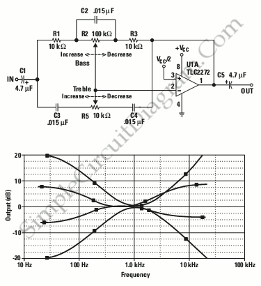
Single Op-Amp Tone Control
This is a single operational amplifier tone control circuit. The circuit functions as a hybrid low-pass, high-pass, and one-pole filter with both attenuation and gain.
The single op-amp tone control circuit utilizes an operational amplifier (op-amp) to manipulate audio signals by...

Simulator Test Tools Speed Circuit Design
A zero-crossing detector converts an input sine wave (Vin) into a square wave, which, when high, charges an op-amp integrator. A reference-input square wave subsequently discharges the integrator. The output voltage of the integrator at the end of this charge/discharge...