


Summing-amplifier
#summing-amplifier
#op-amp
#CA3193
#BiMOS
#amplifier
#input noise
#gain
#analog circuit
#signal processing

Description: This circuit utilizes a CA3193 BiMOS operational amplifier. The input noise of the amplifier is influenced by the resistor network formed by Rp, Rl, R2, and R3. The gain provided by a single input channel is determined by the ratio of Rp to Rl. To achieve optimal noise performance, it is advisable to minimize the number of input channels used.
The CA3193 BiMOS operational amplifier is characterized by its low input noise and high-speed performance, making it suitable for various applications requiring precision signal amplification. The circuit design emphasizes the importance of resistor selection in managing input noise. The resistors Rp and Rl form a voltage divider that sets the gain for the selected input channel, while R2 and R3 may be used for feedback or additional gain control.
In this configuration, the input noise is a function of the parallel combination of Rl, R2, and R3, which can increase the overall noise level if not carefully managed. Therefore, to enhance the signal-to-noise ratio, it is recommended to keep the number of active input channels to a minimum. This approach not only reduces complexity but also helps maintain the integrity of the signal by limiting the contributions of extraneous noise sources.
For practical implementation, attention should be given to the layout of the circuit to minimize parasitic capacitances and inductances that may affect performance. Additionally, power supply decoupling capacitors should be employed near the op-amp to ensure stable operation and further reduce noise. Overall, the design should aim for a balance between gain, bandwidth, and noise performance to achieve the desired application objectives.This circuit uses a CA3193 BiMOS op amp. Because input noise of the amplifier is increased by Rp/ Rl//R2/ /R3, and the gain that a single input will amplify is the gain of only one of the input channels (Rp/ Rl), for good noise performance, use the smallest number of inputs.
The CA3193 BiMOS operational amplifier is characterized by its low input noise and high-speed performance, making it suitable for various applications requiring precision signal amplification. The circuit design emphasizes the importance of resistor selection in managing input noise. The resistors Rp and Rl form a voltage divider that sets the gain for the selected input channel, while R2 and R3 may be used for feedback or additional gain control.
In this configuration, the input noise is a function of the parallel combination of Rl, R2, and R3, which can increase the overall noise level if not carefully managed. Therefore, to enhance the signal-to-noise ratio, it is recommended to keep the number of active input channels to a minimum. This approach not only reduces complexity but also helps maintain the integrity of the signal by limiting the contributions of extraneous noise sources.
For practical implementation, attention should be given to the layout of the circuit to minimize parasitic capacitances and inductances that may affect performance. Additionally, power supply decoupling capacitors should be employed near the op-amp to ensure stable operation and further reduce noise. Overall, the design should aim for a balance between gain, bandwidth, and noise performance to achieve the desired application objectives.This circuit uses a CA3193 BiMOS op amp. Because input noise of the amplifier is increased by Rp/ Rl//R2/ /R3, and the gain that a single input will amplify is the gain of only one of the input channels (Rp/ Rl), for good noise performance, use the smallest number of inputs.

Amplifier Compressor MC3340P
The output is rectified, and TR2 controls the gain of the ICL. This audio compressor circuit uses an MC3340P as a variable gain amplifier.
The audio compressor circuit described utilizes an MC3340P integrated circuit, which functions as a variable gain amplifier...
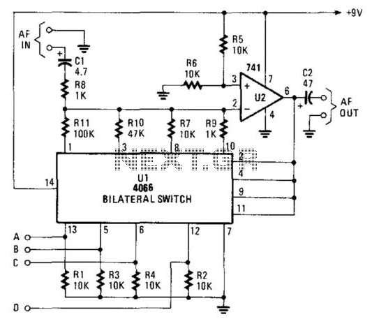
Gain-Controlled Op Amp
The gain controller utilizes a 4066 quad bilateral switch to electronically select a feedback resistor for the 741 operational amplifier. One or more switches can be activated simultaneously to achieve a stepped, variable-gain range from less than 1 to 100.
The...

IC4030-4031 Typical Operating Circuit Schematic and Datasheet
The diagram below illustrates a typical operating circuit for the video line driver using the IC4030/4031 schematic. It incorporates the MAX4030E/MAX4031E, which are unity-gain stable operational amplifiers that offer high-speed performance, rail-to-rail outputs, and 15kV ESD protection, as stated in...

Voltage Controlled Voltage Source
The drawback of the circuit mentioned is that the operational amplifier (op-amp) supply is connected to the high voltage (HV) supply. Most op-amps are limited to approximately 30V for their supply voltage, which prevents the circuit from functioning with higher...
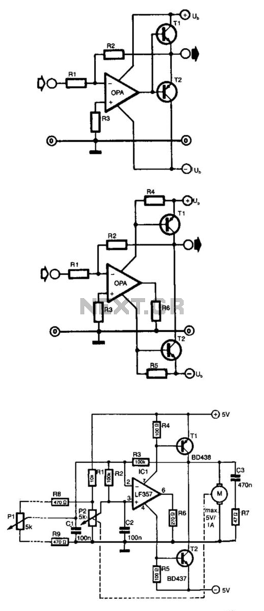
Op Amp Power Driver
Frequently, the output current of an operational amplifier is inadequate for applications such as driving a small motor or loudspeaker. This issue is typically resolved by adding an emitter follower to the circuit. However, this configuration does not allow the...

Op-Amp Circuit: Differentiator
This is a differentiator circuit. This circuit can be used to perform differential operations. There are two types of differentiators: the true differentiator and another type.
A differentiator circuit is designed to output a voltage that is proportional to the rate...

3 Band Graphic Equalizer
This simple equalizer utilizes a single operational amplifier (op-amp) and provides three frequency ranges: low frequency, mid frequency, and high frequency. With the specified component values, it achieves approximately ±20 dB of gain or attenuation at frequencies of 50 Hz,...

Triangle / Squarewave Generators
A simple triangle and square wave generator utilizing a common 1458 dual op-amp, capable of operating from very low frequencies up to approximately 10 kHz. The time interval for one half-cycle is determined by the product of resistance (R) and...

Track-and-hold-sample-and-hold
Channel 1 is configured as a voltage follower and is activated during the track/sample time. If the product of R and C is sufficiently short compared to the period of maximum output frequency or sample time, then C will charge...