


50Mhz-trigger

Description: This circuit features a stable trigger with a sensitivity of 100 mV at 50 MHz. It utilizes FETs to create a high-speed buffer, while the LT1016 compares the output of this buffer to the voltage at the trigger level potentiometer, which can be configured for either polarity. A 10 kΩ resistor introduces hysteresis, effectively eliminating chattering caused by noisy input signals. To calibrate the circuit, the input should be grounded, and the input zero control should be adjusted to achieve 0 V at the drain terminal of Q2.
This circuit is designed for high-frequency applications requiring precise triggering capabilities. The 100 mV sensitivity at 50 MHz indicates that it can accurately respond to small voltage changes, making it suitable for environments where signal integrity is critical. The use of FETs provides a high-speed buffer that minimizes signal degradation, ensuring that the output remains faithful to the input signal.
The LT1016 operational amplifier serves as a comparator in this setup, allowing for the comparison of the buffered signal against a user-defined threshold set by the trigger level potentiometer. The inclusion of a potentiometer that can be configured for either polarity adds flexibility to the circuit, enabling it to adapt to various signal conditions and requirements.
The 10 kΩ resistor plays a crucial role in enhancing the circuit's performance by introducing hysteresis. This feature is particularly important in noisy environments, where rapid fluctuations in the input signal can lead to false triggering or chattering. By providing a defined threshold for switching, the hysteresis ensures that the circuit operates reliably, even in the presence of noise.
Calibration is a straightforward process. By grounding the input, the circuit can be adjusted to ensure that the output reflects a true zero voltage level at the drain terminal of Q2. This step is essential for maintaining accuracy and reliability in the circuit's operation, ensuring that it functions as intended across a range of conditions. Overall, this circuit design is effective for applications that require reliable triggering in high-frequency environments.This has a stable trigger 100 m V sensitivity at 50 MHz. The FETs comprise a simple high-speed buffer and the LT1016 compares the buffer"s output to the potential at tbe trigger level potentiometer, which can be of either polarity. The 10-KO resistor provides hysteresis, eliminating "chattering"" caused by noisy input signals. To calibrate this circuit, ground the input and adjust the input zero control for 0 V at Q2"s drain terminal.
This circuit is designed for high-frequency applications requiring precise triggering capabilities. The 100 mV sensitivity at 50 MHz indicates that it can accurately respond to small voltage changes, making it suitable for environments where signal integrity is critical. The use of FETs provides a high-speed buffer that minimizes signal degradation, ensuring that the output remains faithful to the input signal.
The LT1016 operational amplifier serves as a comparator in this setup, allowing for the comparison of the buffered signal against a user-defined threshold set by the trigger level potentiometer. The inclusion of a potentiometer that can be configured for either polarity adds flexibility to the circuit, enabling it to adapt to various signal conditions and requirements.
The 10 kΩ resistor plays a crucial role in enhancing the circuit's performance by introducing hysteresis. This feature is particularly important in noisy environments, where rapid fluctuations in the input signal can lead to false triggering or chattering. By providing a defined threshold for switching, the hysteresis ensures that the circuit operates reliably, even in the presence of noise.
Calibration is a straightforward process. By grounding the input, the circuit can be adjusted to ensure that the output reflects a true zero voltage level at the drain terminal of Q2. This step is essential for maintaining accuracy and reliability in the circuit's operation, ensuring that it functions as intended across a range of conditions. Overall, this circuit design is effective for applications that require reliable triggering in high-frequency environments.This has a stable trigger 100 m V sensitivity at 50 MHz. The FETs comprise a simple high-speed buffer and the LT1016 compares the buffer"s output to the potential at tbe trigger level potentiometer, which can be of either polarity. The 10-KO resistor provides hysteresis, eliminating "chattering"" caused by noisy input signals. To calibrate this circuit, ground the input and adjust the input zero control for 0 V at Q2"s drain terminal.

MPF102 FET Preamplifier
The circuit described is a single JFET design that provides limited gain. By incorporating a source resistor bypass capacitor, the gain can be significantly enhanced, resembling a single stage of the original tube preamp used in guitar amplifiers. It is...

50Mhz-vhf-crystal-oscillator
The diagram illustrates a 50 MHz oscillator functioning at its third harmonic. The collector load resistor R1 has been increased due to the rise in the quartz crystal's internal series resistance Rs, which escalates with frequency in the VHF range....

FETVM-FET Voltmeter
This is a circuit of a FETVM (Field Effect Transistor Voltmeter). The function of the VTVM (Vacuum Tube Voltmeter) is replaced by the FETVM while eliminating the conventional line cord instrument.
The FETVM circuit employs field effect transistors (FETs) to measure...
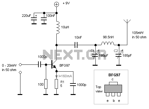
50MHz Linear Power Amplifier
This page investigates a simple PA for 50MHz. This power amplifier will boost a low-level signal about 10-20mW to over 100mW. The power consumption will yet be quite low. At the bottom of this page, a complete transmitter based on...

FET Colpitts Oscillator (Microwave)
A 430 MHz transmitter for microwave applications is being constructed, but there is an issue with obtaining any output frequency from the circuit.
The construction of a 430 MHz transmitter for microwave applications involves several critical components and considerations to ensure...

FET VOLTMETER
The 2N3819 FET serves as a solid-state voltage output meter (VOM). In this configuration, the 2N3819 functions as a cathode follower. The bias offset, or meter null, is achieved using resistors R14 and R12, while the full-scale calibration is set...

FET Preamp with LND150
The saturation region begins at the knees on the left side. This analysis focuses on curves for negative gate voltages, indicating depletion mode operation. It is important to note that the device can also function in enhancement mode with positive...

FET Cascode Video Amplifier
This circuit is a FET Cascode Video Amplifier. The cascode amplifier FET used for video applications has a very low input impedance and nearly zero feedback reduction. The 2N3823 transistor was selected due to its low capacitance and high transconductance...

FET biasing
Unlike BJTs, thermal runaway does not occur with FETs. However, the significant differences in maximum and minimum transfer characteristics make ID levels unpredictable with a simple fixed-gate bias voltage. To achieve reasonable limits on quiescent drain currents (ID) and drain-source...