


Low-Frequency Crystal Oscillator Circuit
#low-frequency
#crystal oscillator
#astable multivibrator
#field effect transistor
#sine wave
#wideband operation
#resistive load

Description: Q1, Q2, and the associated circuitry constitute a modified astable multivibrator where the loop gain is automatically adjusted to the threshold of oscillation by field effect transistor Q3. Q4 amplifies the signal at the collector of Q2 and isolates the oscillator section from the output. This stage operates over a wide bandwidth and provides a clean 2.5-V amplitude sine wave into a resistive load of 20 kΩ or greater. The stage containing Q5 has a voltage gain of 1 and is designed to isolate the nonlinear effects of rectifier D1 from the output.
The described circuit employs a modified astable multivibrator configuration using transistors Q1 and Q2 to generate oscillations. The automatic adjustment of the loop gain to the oscillation threshold is facilitated by field effect transistor Q3, which plays a critical role in maintaining stable oscillation conditions. This automatic gain control ensures that the circuit remains operational across varying load conditions and environmental factors.
Transistor Q4 serves as a linear amplifier, taking the output signal from the collector of Q2. Its primary function is to amplify the oscillatory signal while also providing isolation between the oscillator and the subsequent output stage. This isolation is essential to prevent feedback that could destabilize the oscillator. The output from Q4 is characterized by a clean sine wave with an amplitude of 2.5 V, making it suitable for driving resistive loads of 20 kΩ or higher. The wideband operation of this stage indicates that the circuit can effectively handle a range of frequencies without significant distortion, which is crucial for applications requiring high fidelity in signal reproduction.
The inclusion of transistor Q5, which operates with a voltage gain of 1, ensures that the output is not influenced by the nonlinear characteristics of rectifier D1. This isolation is important as it preserves the integrity of the output signal, allowing for accurate signal processing downstream without introducing unwanted distortions from the rectification process. Overall, the circuit is designed to provide reliable oscillation, effective amplification, and signal integrity, making it suitable for various electronic applications. Ql, Q2, and the associated circuitry form a modified astable multivibrator in which the loop gain is automatically adjusted to the threshold of oscillation by means of field effect transistor Q3. Q4 linearly amplifies the signal present at the collector of Q2 and isolates the oscillator section of the circuit from the output.
This stage features wideband operation and delivers a clean 2.5-V amplitude sine wave into a resistive load greater than or equal to 20 kQ. The stage comprising Q5 has a voltage gain of 1 and its sole purpose is to isolate the nonlinear effects of rectifier D1 from the output.
The described circuit employs a modified astable multivibrator configuration using transistors Q1 and Q2 to generate oscillations. The automatic adjustment of the loop gain to the oscillation threshold is facilitated by field effect transistor Q3, which plays a critical role in maintaining stable oscillation conditions. This automatic gain control ensures that the circuit remains operational across varying load conditions and environmental factors.
Transistor Q4 serves as a linear amplifier, taking the output signal from the collector of Q2. Its primary function is to amplify the oscillatory signal while also providing isolation between the oscillator and the subsequent output stage. This isolation is essential to prevent feedback that could destabilize the oscillator. The output from Q4 is characterized by a clean sine wave with an amplitude of 2.5 V, making it suitable for driving resistive loads of 20 kΩ or higher. The wideband operation of this stage indicates that the circuit can effectively handle a range of frequencies without significant distortion, which is crucial for applications requiring high fidelity in signal reproduction.
The inclusion of transistor Q5, which operates with a voltage gain of 1, ensures that the output is not influenced by the nonlinear characteristics of rectifier D1. This isolation is important as it preserves the integrity of the output signal, allowing for accurate signal processing downstream without introducing unwanted distortions from the rectification process. Overall, the circuit is designed to provide reliable oscillation, effective amplification, and signal integrity, making it suitable for various electronic applications. Ql, Q2, and the associated circuitry form a modified astable multivibrator in which the loop gain is automatically adjusted to the threshold of oscillation by means of field effect transistor Q3. Q4 linearly amplifies the signal present at the collector of Q2 and isolates the oscillator section of the circuit from the output.
This stage features wideband operation and delivers a clean 2.5-V amplitude sine wave into a resistive load greater than or equal to 20 kQ. The stage comprising Q5 has a voltage gain of 1 and its sole purpose is to isolate the nonlinear effects of rectifier D1 from the output.

digital sine wave synthesis
In an analog world, converting digital values to their analog equivalents is often necessary when using microcontrollers. Many low-cost microcontrollers lack built-in hardware digital-to-analog converters (DACs), but most feature an 8-bit or 16-bit timer capable of generating Pulse Width Modulation...
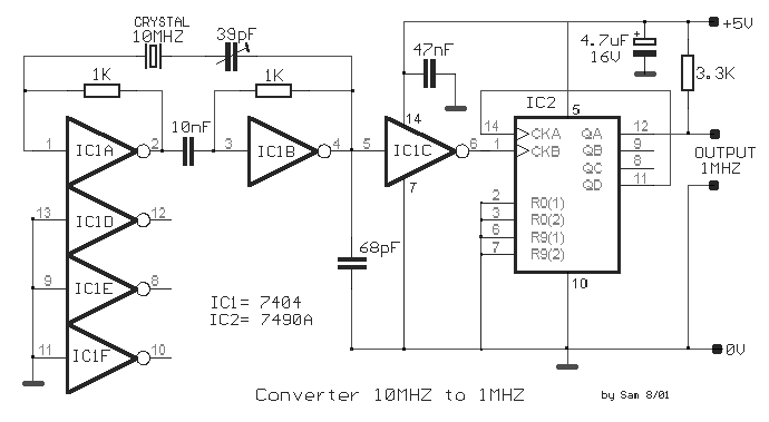
Crystal Oscillator Frequency Converter
The circuit was designed to create a frequency converter using a crystal oscillator for the conversion of 10 MHz to 1 MHz. It incorporates a 7404 hex inverter.
The circuit functions as a frequency divider, utilizing a crystal oscillator to generate...

Crystal Oscillators
The circuit is designed exclusively for fundamental crystals, as it lacks mode suppression components. The oscillator transistor Q104 remains in a cutoff state for most of the time, activating only briefly during the peak of the crystal current waveform. Transistor...

12vdc to 220vac inverter with sine wave output
In DA3, DA5, VT1, and VT2, the first channel of the VLF Class D amplifier is assembled. The second channel is constructed using DA4, DA7, VT3, and VT4. Antiphase sine waves in the VLF range are formed at the outputs...

how to get more power out of a astable multivibrator
Powering this circuit with a 6V alkaline battery operates effectively with 100µF capacitors. However, there is an issue when attempting to replace the LED with a DPDT relay; a 6V relay previously available does not activate. Additionally, when using a...

Wien bridge sine wave oscillator circuit composed of LM101A
The chart illustrates the Wien bridge sine wave oscillator circuit. The amount of negative feedback in the circuit is determined by the internal resistance of the FET. When the peak output voltage of the oscillator reaches the regulated voltage of...

Integrated-am-receiver
A crystal oscillator is used so that a narrow-band hybrid IF filter can be utilized. This circuit includes aerial and local oscillator circuits for a 27-MHz receiver, intended for the remote control of garage doors, projectors, curtains, and similar applications.
The...

Low-frequency-transmitter
The crystal oscillator utilizes two sections of IC1, a 4001 quad 2-input NOR gate, representing a standard and reliable design. The oscillator generates a 1.85-MHz square-wave output that feeds into IC2, a 4017 divide-by-10 counter. The count enable and reset...

Low-frequency-pierce-oscillator
The Pierce circuit oscillates at 4 kHz. At low frequencies, the crystal's internal series resistance Rs is quite high (45 kΩ at 4 kHz). Therefore, an FET-based source follower is included to prevent Q1 from loading the crystal output.
The Pierce...