


VCO with NE567
#VCO
#NE567
#PLL
#audio tone decoder
#sidetone oscillator
#amateur radio
#triangle signal
#square wave signal


Description: Who would like to build a sidetone oscillator with a minimum amount of parts should try the NE567 integrated circuit. The NE567 is a PLL circuit with an internal VCO for a operating frequency less than 500 kHz and it is normally used as an audio tone decoder. The VCO frequency is adjustable by two passive components only. For a 750 Hz sidetone in an amateur radio application the capacitor C1 and the resistor R1 define the VCO frequency. The IC supplier allows for R1 a range of 2 .... 20 kOhm. The sidetone can be taken from pin 6 as a symmetrical triangle signal or as a high impedance square wave signal from pin 5. The triangle signal has an amplitude of 1 Vss and the square wave signal of 2 Vss. In order to switch on the oscillator during transmit mode Tx, one can connect pin 7 to Gnd or pin 4 to Vcc. Pins 1, 2, 3 and 8 remain free (nc). The permissible supply voltage Vcc is +4 V to +10 V. With about 6 mA at Vcc = +5 V the IC is relatively economically in its current consumption. The second sidetone oscillator is built up completely discrete with two transistors and four passive components. The VT1 and VT2 arrangement corresponds to the thyristor substitute circuit, but with something special. Not the emitter of VT2 but the VT2 collector is connected to Gnd potential. If one runs VT2 as usual with the emitter connected to ground, VT1 and VT2 together have a very high current gain. This high gain causes that the low current flow through R1 (C1 is discharged via VT1) is sufficient high that both transistors remain in the on state. Hence periodically charging and discharging the capacitor is impossible, because the hold on current will never be fallen below. A measure against this effect could be a low impedance voltage divider R2/R3 in order to take over a partial current (Ic_VT2) or a gain reduction. The later is achieved very easy with the reverse operation of VT2. The hold on current is fallen and thus VT1 and VT2 return to the off state after discharging C1. Now the circuit operates as planned. C1 will be charged by a low current via R1 up to the voltage rate Uc = Ux + 0,7 V. A small basis current flows into VT1 as soon as Uc exceeds the limit value Ux + 0,7 V. VT2 conducts too by the now starting collector current. On the basis of the positive feedback both transistors are conducting quickly and VT2 discharges the capacitor immediately. The collector current defined by R1 is lower than the hold on current required for VT1 and VT2. Both transistors go back to the non-conducting state and the game starts from the beginning. The advantage of the circuit is the excellent frequency stability a supply voltage changes. If the supply voltage decreases the charging time of C1 rises and thus the frequency. Because the limit value Ux decreases at the same time the frequency rises thereupon. The achievable compensation with the specified components within the voltage range Us = +7 ... +15 V is nearly perfect. The difference to the 650 Hz nominal frequency is only +/- 5 Hz. At 2 V supply voltage the saw tooth signal amplitude at the output is 2,5 Vss. The Tx control signal can not only switch off and on the complete circuit but it can also supply it due to the low current consumption of less than 0,5 mA. The Us terminal is not necessary then.
The NE567 integrated circuit serves as the core component for constructing a sidetone oscillator, particularly suitable for applications requiring minimal parts. This phase-locked loop (PLL) circuit incorporates an internal voltage-controlled oscillator (VCO) capable of operating at frequencies below 500 kHz, primarily designed for audio tone decoding. The frequency of the VCO is determined by two external passive components: a capacitor (C1) and a resistor (R1). For achieving a desired sidetone frequency of 750 Hz, R1 can be selected within the range of 2 kΩ to 20 kΩ as specified by the manufacturer.
The sidetone output can be accessed from pin 6, providing a symmetrical triangle waveform with an amplitude of 1 V peak-to-peak (Vpp), or from pin 5, delivering a high-impedance square wave signal with an amplitude of 2 Vpp. To activate the oscillator during transmission mode (Tx), pin 7 can be connected to ground (Gnd) or pin 4 to the supply voltage (Vcc), while pins 1, 2, 3, and 8 are left unconnected (nc).
The operational voltage range for Vcc is between +4 V and +10 V, with a current consumption of approximately 6 mA at Vcc = +5 V, making the circuit relatively power-efficient. An alternative sidetone oscillator design can be implemented using discrete components, specifically two transistors (VT1 and VT2) and four passive components. This configuration resembles a thyristor substitute circuit, with the unique aspect that the collector of VT2 is connected to ground rather than the emitter.
In this discrete configuration, the high current gain of the transistor pair VT1 and VT2 allows for a low current through R1 to maintain both transistors in the conducting state. Consequently, the periodic charging and discharging of capacitor C1 is hindered, as the hold current remains above the threshold. To mitigate this effect, a low-impedance voltage divider (R2/R3) can be introduced to siphon off a portion of the current, or a gain reduction can be achieved by reversing the operation of VT2, allowing for the transistors to turn off after discharging C1.
The circuit operates effectively by charging C1 through R1 until the voltage across C1 reaches Uc = Ux + 0.7 V. When this threshold is surpassed, a small base current activates VT1, leading to VT2 also conducting due to the resulting collector current. This positive feedback mechanism rapidly turns both transistors on, causing VT2 to discharge C1. As the collector current defined by R1 is less than the hold current needed for both transistors, they eventually return to the off state, repeating the cycle.
The circuit's design offers excellent frequency stability in response to variations in supply voltage. A decrease in supply voltage results in an increased charging time for C1, consequently raising the output frequency. The compensation achieved with the specified components within the voltage range of +7 V to +15 V is nearly flawless, maintaining a deviation of only +/- 5 Hz from the nominal frequency of 650 Hz. At a supply voltage of 2 V, the output sawtooth signal amplitude reaches 2.5 Vpp. Moreover, the Tx control signal not only enables and disables the entire circuit but also powers it, given the low current consumption of less than 0.5 mA, rendering the Us terminal unnecessary in this configuration.Who would like to build a sidetone oscillator with a minimum amount of parts should try the NE567 integrated circuit. The NE567 is a PLL circuit with an internal VCO for a operating frequency less than 500 kHz and it is normally used as an audio tone decoder.
The VCO frequency is adjustable by two passive components only. For a 750 Hz sidetone in an amateur radio application the capacitor C1 and the resistor R1 define the VCO frequency. The IC supplier allows for R1 a range of 2 .... 20 kOhm. The sidetone can be taken from pin 6 as a symmetrical triangle signal or as a high impedance square wave signal from pin 5.
The triangle signal has an amplitude of 1 Vss and the square wave signal of 2 Vss. In order to switch on the oscillator during transmit mode Tx, one can connect pin 7 to Gnd or pin 4 to Vcc. Pins 1, 2, 3 and 8 remain free (nc). The permissible supply voltage Vcc is +4 V to +10 V. With about 6 mA at Vcc = +5 V the IC is relatively economically in its current consumption. The second sidetone oscillator is build up completely discrete with two transistors and four passive components. The VT1 and VT2 arrangement corresponds to the thyristor substitute circuit, but with something special.
Not the emitter of VT2 but the VT2 collector is connected to Gnd potential. If one runs VT2 as usual with the emitter connected to ground, VT1 and VT2 together have a very high current gain. This high gain causes that the low current flow through R1 (C1 is discharged via VT1) is sufficient high that both transistors remain in the on state.
Hence periodically charging and discharging the capacitor is impossible, because the hold on current will never be fallen below. A measure against this effect could be a low impedance voltage divider R2/R3 in order to take over a partial current (Ic_VT2) or a gain reduction.
The later is achieved very easy with the reverse operation of VT2. The hold on current is fallen and thus VT1 and VT2 return to the off state after discharging C1. Now the circuit operates as planed. C1 will be charged by a low current via R1 up to the voltage rate Uc = Ux + 0,7 V. A small basis current flows into VT1 as soon as Uc exceeds the limit value Ux + 0,7 V. VT2 conducts too by the now starting collector current. On the basis of the positive feedback both transistors are conducting quickly and VT2 discharges the capacitor immediately. The collector current defined by R1 is lower than the hold on current required for VT1 and VT2. Both transistors go back to the non-conducting state and the game starts from the beginning. The advantage of the circuit is the excellent frequency stability a supply voltage changes. If the supply voltage decreases the charging time of C1 rises and thus the frequency. Because the limit value Ux decreases at the same time the frequency rises thereupon. The achievable compensation with the specified components within the voltage range Us = +7 ... +15 V is nearly perfect. The difference to the 650 Hz nominal frequency is only +/- 5 Hz. At 2 V supply voltage the saw tooth signal amplitude at the output is 2,5 Vss. The Tx control signal can not only switch off and on the the complete circuit but it can also supply it due to the low current consumption of less than 0,5 mA.
The Us terminal is not necessary then.
The NE567 integrated circuit serves as the core component for constructing a sidetone oscillator, particularly suitable for applications requiring minimal parts. This phase-locked loop (PLL) circuit incorporates an internal voltage-controlled oscillator (VCO) capable of operating at frequencies below 500 kHz, primarily designed for audio tone decoding. The frequency of the VCO is determined by two external passive components: a capacitor (C1) and a resistor (R1). For achieving a desired sidetone frequency of 750 Hz, R1 can be selected within the range of 2 kΩ to 20 kΩ as specified by the manufacturer.
The sidetone output can be accessed from pin 6, providing a symmetrical triangle waveform with an amplitude of 1 V peak-to-peak (Vpp), or from pin 5, delivering a high-impedance square wave signal with an amplitude of 2 Vpp. To activate the oscillator during transmission mode (Tx), pin 7 can be connected to ground (Gnd) or pin 4 to the supply voltage (Vcc), while pins 1, 2, 3, and 8 are left unconnected (nc).
The operational voltage range for Vcc is between +4 V and +10 V, with a current consumption of approximately 6 mA at Vcc = +5 V, making the circuit relatively power-efficient. An alternative sidetone oscillator design can be implemented using discrete components, specifically two transistors (VT1 and VT2) and four passive components. This configuration resembles a thyristor substitute circuit, with the unique aspect that the collector of VT2 is connected to ground rather than the emitter.
In this discrete configuration, the high current gain of the transistor pair VT1 and VT2 allows for a low current through R1 to maintain both transistors in the conducting state. Consequently, the periodic charging and discharging of capacitor C1 is hindered, as the hold current remains above the threshold. To mitigate this effect, a low-impedance voltage divider (R2/R3) can be introduced to siphon off a portion of the current, or a gain reduction can be achieved by reversing the operation of VT2, allowing for the transistors to turn off after discharging C1.
The circuit operates effectively by charging C1 through R1 until the voltage across C1 reaches Uc = Ux + 0.7 V. When this threshold is surpassed, a small base current activates VT1, leading to VT2 also conducting due to the resulting collector current. This positive feedback mechanism rapidly turns both transistors on, causing VT2 to discharge C1. As the collector current defined by R1 is less than the hold current needed for both transistors, they eventually return to the off state, repeating the cycle.
The circuit's design offers excellent frequency stability in response to variations in supply voltage. A decrease in supply voltage results in an increased charging time for C1, consequently raising the output frequency. The compensation achieved with the specified components within the voltage range of +7 V to +15 V is nearly flawless, maintaining a deviation of only +/- 5 Hz from the nominal frequency of 650 Hz. At a supply voltage of 2 V, the output sawtooth signal amplitude reaches 2.5 Vpp. Moreover, the Tx control signal not only enables and disables the entire circuit but also powers it, given the low current consumption of less than 0.5 mA, rendering the Us terminal unnecessary in this configuration.Who would like to build a sidetone oscillator with a minimum amount of parts should try the NE567 integrated circuit. The NE567 is a PLL circuit with an internal VCO for a operating frequency less than 500 kHz and it is normally used as an audio tone decoder.
The VCO frequency is adjustable by two passive components only. For a 750 Hz sidetone in an amateur radio application the capacitor C1 and the resistor R1 define the VCO frequency. The IC supplier allows for R1 a range of 2 .... 20 kOhm. The sidetone can be taken from pin 6 as a symmetrical triangle signal or as a high impedance square wave signal from pin 5.
The triangle signal has an amplitude of 1 Vss and the square wave signal of 2 Vss. In order to switch on the oscillator during transmit mode Tx, one can connect pin 7 to Gnd or pin 4 to Vcc. Pins 1, 2, 3 and 8 remain free (nc). The permissible supply voltage Vcc is +4 V to +10 V. With about 6 mA at Vcc = +5 V the IC is relatively economically in its current consumption. The second sidetone oscillator is build up completely discrete with two transistors and four passive components. The VT1 and VT2 arrangement corresponds to the thyristor substitute circuit, but with something special.
Not the emitter of VT2 but the VT2 collector is connected to Gnd potential. If one runs VT2 as usual with the emitter connected to ground, VT1 and VT2 together have a very high current gain. This high gain causes that the low current flow through R1 (C1 is discharged via VT1) is sufficient high that both transistors remain in the on state.
Hence periodically charging and discharging the capacitor is impossible, because the hold on current will never be fallen below. A measure against this effect could be a low impedance voltage divider R2/R3 in order to take over a partial current (Ic_VT2) or a gain reduction.
The later is achieved very easy with the reverse operation of VT2. The hold on current is fallen and thus VT1 and VT2 return to the off state after discharging C1. Now the circuit operates as planed. C1 will be charged by a low current via R1 up to the voltage rate Uc = Ux + 0,7 V. A small basis current flows into VT1 as soon as Uc exceeds the limit value Ux + 0,7 V. VT2 conducts too by the now starting collector current. On the basis of the positive feedback both transistors are conducting quickly and VT2 discharges the capacitor immediately. The collector current defined by R1 is lower than the hold on current required for VT1 and VT2. Both transistors go back to the non-conducting state and the game starts from the beginning. The advantage of the circuit is the excellent frequency stability a supply voltage changes. If the supply voltage decreases the charging time of C1 rises and thus the frequency. Because the limit value Ux decreases at the same time the frequency rises thereupon. The achievable compensation with the specified components within the voltage range Us = +7 ... +15 V is nearly perfect. The difference to the 650 Hz nominal frequency is only +/- 5 Hz. At 2 V supply voltage the saw tooth signal amplitude at the output is 2,5 Vss. The Tx control signal can not only switch off and on the the complete circuit but it can also supply it due to the low current consumption of less than 0,5 mA.
The Us terminal is not necessary then.

CDCF5801 Low Jitter PLL Based Multiplier/Divider With Programmable Delay Lines Down To Sub 10ps
The CF5019 series are high-frequency, third overtone crystal oscillator module ICs. They integrate an oscillator circuit and an output buffer that function at high frequencies on a single chip. The oscillator circuit utilizes CMOS inverters and a built-in damping resistor...

Simple Audio-Frequency Vco
The frequency of this sine-wave oscillator is determined by a direct voltage, U, ranging from 0 to 15 V. The distortion in output signals of up to 10 Vpp does not exceed 1%. When the output is reduced using P1...

vcd
This module was originally developed as a timing accessory for a sequencer. When connected to a Voltage-Controlled Oscillator (VCO), it can produce interesting frequency trills reminiscent of old 8-bit computer games. Feeding the control voltage from a Psycho Low-Frequency Oscillator...
The Second W9VES
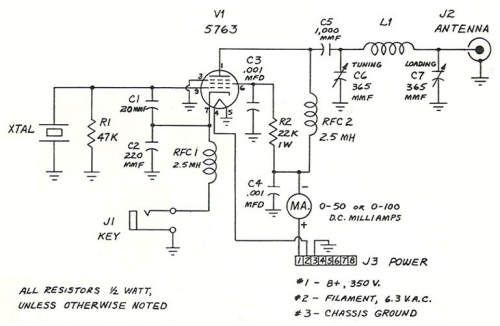
The amateur radio call sign W9VES has been assigned to only two individuals, of whom the second is the author. The first holder was the author's maternal uncle, Phil Simmons, and the author enjoys amateur radio in his memory. By...

The PLL FM demodulator (4046) circuit
The FM demodulator circuit, as illustrated in the figure, utilizes a 4046 Phase-Locked Loop (PLL) integrated circuit to convert the intermediate frequency FM input signal into a lower frequency output.
The FM demodulator circuit based on the 4046 PLL IC operates...

PLL FM Demodulator
A Phase Locked Loop (PLL) can be utilized to create a Frequency Modulation (FM) demodulator. The PLL circuit tracks the input frequency by adjusting the voltage input of a Voltage-Controlled Oscillator (VCO).
The Phase Locked Loop (PLL) is a critical component...

PLL FM Transmitter using LMX1601 ATtiny2313 AT90S2313
This document describes a PLL FM transmitter utilizing the LMX1601 and either the ATtiny2313 or AT90S2313 microcontrollers. A common feature of previous low-power FM transmitters developed over the years is that their operating frequency is determined by an LC resonant...

Simple-vco
The output frequency of the voltage-controlled oscillator (VCO), U1, varies inversely with the input voltage. With a 1 V input, the oscillator output frequency is approximately 1500 Hz; with a 5 V input, the output frequency decreases to around 300...
LINEAR VCO
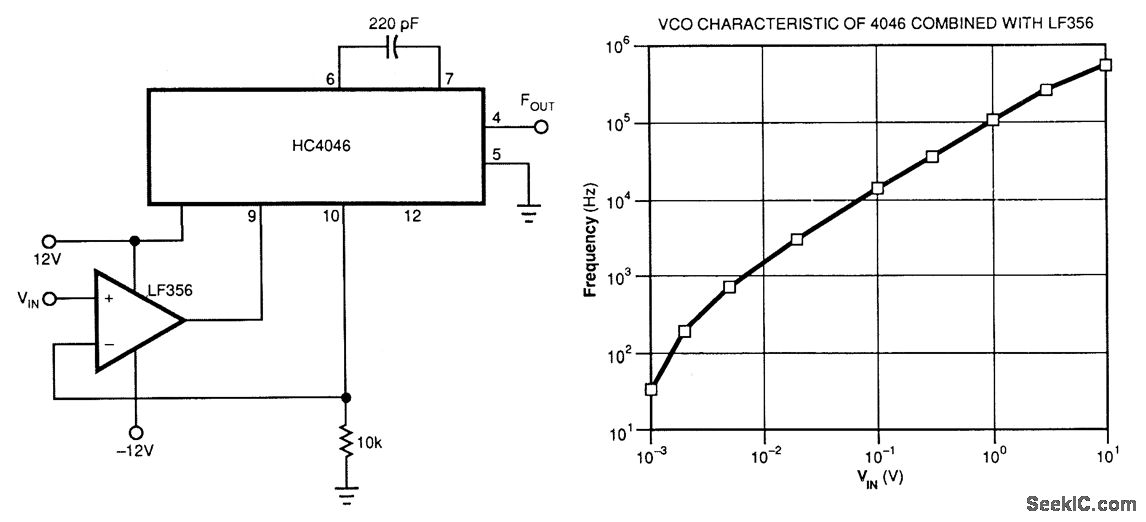
This voltage-controlled oscillator (VCO) utilizes an LF356 operational amplifier to generate a linear frequency versus voltage characteristic in conjunction with the CMOS HC4046. The frequency range can be adjusted by modifying the capacitor linked between pins 6 and 7 of...