


DDR memory power supply circuit

Description: DDR memory power supply circuit. This circuit illustrates the power supply configuration for notebook DDR memory, utilizing the MAX8632 power control circuit chip. The power supply terminal VDD is connected to the voltage detection point 1. The battery DC supply voltage ranges from 4.5 V to 2.8 V. The switching voltage is applied to the drain of the field effect transistor Q1, while the DH and DL outputs of the control chip generate PWM pulse signals that are out of phase. These signals are directed to the gates of transistors Q1 and Q2. As a result of the PWM pulse action, Q1 and Q2 operate alternately, converting the DC battery voltage into a switching voltage. This voltage is then processed through an LC filter to yield an output voltage of 2.5 V for the memory circuitry.
The DDR memory power supply circuit is designed to efficiently convert a variable DC battery voltage into a stable output voltage suitable for DDR memory operation. The MAX8632 chip serves as the core component of the power control circuit, managing the power supply by generating pulse-width modulation (PWM) signals. These PWM signals are crucial for controlling the switching action of the field effect transistors Q1 and Q2, which are configured in a push-pull arrangement.
The operation begins with the detection of the battery voltage, which can range from 4.5 V to 2.8 V. This range is essential for ensuring compatibility with various battery types and states of charge. The MAX8632 monitors this voltage and adjusts the PWM signals accordingly to maintain the desired output voltage. The switching voltage applied to the drain of Q1 allows for the modulation of the input battery voltage.
Transistors Q1 and Q2 are key components in this circuit, as they alternately conduct based on the PWM signals they receive. When Q1 is turned on, it allows current to flow from the battery through the load, while Q2 is turned off, and vice versa. This complementary operation ensures that the output voltage remains stable despite variations in the input voltage or load conditions.
The LC filter, composed of an inductor (L) and a capacitor (C), smooths the PWM output to produce a consistent 2.5 V output. This filtered voltage is crucial for the reliable operation of DDR memory, which requires a stable power supply to function correctly. The design of the LC filter is critical, as it must effectively reduce ripple voltage while maintaining efficiency.
Overall, this DDR memory power supply circuit exemplifies a robust design that efficiently converts battery voltage to a suitable level for memory applications, ensuring reliable performance in notebook devices.DDR memory power supply circuit Shows the notebook DDR memory power supply circuit, the power control circuit chip MAX8632, the chip power supply terminal VDD is Sv (detection point 1), the battery DC supply voltage between 4.5 V-2.8 V, the the switching voltage is applied to the field effect transistor Ql drain power supply control chip DH, DL outputs a PWM pulse of opposite phase signals, which signals are applied to Ql, Q2 of the gate, under the action of the PWM pulse Q1, Q2 alternately working, the DC voltage of the battery becomes switching voltage, and then after the LC filter output voltage of 2.V for the memory circuitry.
The DDR memory power supply circuit is designed to efficiently convert a variable DC battery voltage into a stable output voltage suitable for DDR memory operation. The MAX8632 chip serves as the core component of the power control circuit, managing the power supply by generating pulse-width modulation (PWM) signals. These PWM signals are crucial for controlling the switching action of the field effect transistors Q1 and Q2, which are configured in a push-pull arrangement.
The operation begins with the detection of the battery voltage, which can range from 4.5 V to 2.8 V. This range is essential for ensuring compatibility with various battery types and states of charge. The MAX8632 monitors this voltage and adjusts the PWM signals accordingly to maintain the desired output voltage. The switching voltage applied to the drain of Q1 allows for the modulation of the input battery voltage.
Transistors Q1 and Q2 are key components in this circuit, as they alternately conduct based on the PWM signals they receive. When Q1 is turned on, it allows current to flow from the battery through the load, while Q2 is turned off, and vice versa. This complementary operation ensures that the output voltage remains stable despite variations in the input voltage or load conditions.
The LC filter, composed of an inductor (L) and a capacitor (C), smooths the PWM output to produce a consistent 2.5 V output. This filtered voltage is crucial for the reliable operation of DDR memory, which requires a stable power supply to function correctly. The design of the LC filter is critical, as it must effectively reduce ripple voltage while maintaining efficiency.
Overall, this DDR memory power supply circuit exemplifies a robust design that efficiently converts battery voltage to a suitable level for memory applications, ensuring reliable performance in notebook devices.DDR memory power supply circuit Shows the notebook DDR memory power supply circuit, the power control circuit chip MAX8632, the chip power supply terminal VDD is Sv (detection point 1), the battery DC supply voltage between 4.5 V-2.8 V, the the switching voltage is applied to the field effect transistor Ql drain power supply control chip DH, DL outputs a PWM pulse of opposite phase signals, which signals are applied to Ql, Q2 of the gate, under the action of the PWM pulse Q1, Q2 alternately working, the DC voltage of the battery becomes switching voltage, and then after the LC filter output voltage of 2.V for the memory circuitry.

Output sampling winding isolated switching power supply
The diagram illustrates the output sampling winding of an isolated switching power supply. In the diagram, T represents a high-frequency transformer; N2 denotes the self-oscillation positive feedback winding; N3 is the error amplifier; VTS is the winding that provides the...

Battery charger or Power Supply 14 volt 4 ampere
The schematic diagram originates from a circuit designed as a battery charger/power supply with an output of 14V and a maximum current of 4A, utilizing the VN64GA MOSFET. This high-performance battery charger is specifically engineered for gelled electrolyte lead-acid batteries,...

power supply circuit
The SheevaPlug is known to have a suboptimal power supply, particularly affecting users in the UK operating at 240VAC. Additionally, heavy loads on the USB can cause issues, especially when connecting an external mechanical disk drive. This project aims to...
Circuit diagrams and Schematic
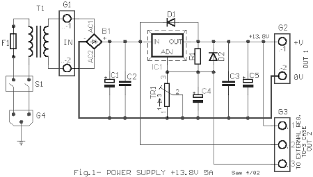
This AC to DC power supply can output 5A in continuous operation and 12A peak current. This type of DC power supply uses a PCB, allowing for two case types for IC1: TO-220 or TO-3. The regulation of this 12-volt...

FSP107-2PS01 two-in-one power panel circuit analysis
The main component is the LG26 one-inch screens integrated with the FSP107-2PS01 two-in-one electrical power package, which utilizes a direct drive CCFL modulator tube. This setup is compatible with screens from other manufacturers, such as Samsung and AU, but requires...

power How can I switch a high current with a low-rated switch
The project involves designing and constructing a breadboard power supply that draws power from an ATX-like switch-mode power supply (SMPS) using a 4-pin Molex connector. The design features a switch to select either a 12V or 5V output. However, the...

psu
The Chameleon II Power Supply Circuits convert the raw input supply into stable voltage outputs necessary for the Chameleon interfaces. The outputs provided are +5V, +12V, and -12V.
The Chameleon II Power Supply Circuits are designed to ensure reliable operation of...

250 Watt PC power Supply
Up to 10 A continuous output current, or operation with 50 % ESD and 18 A peak current are possible without a fan if sufficient natural air flow is present and the ambient temperature does not exceed 30 °C. A...

A typical DVD switching power supply circuit
A typical DVD switching power supply circuit is shown in the standby power supply circuit of digital products. It utilizes a switching power supply structure, with the oscillation switch IC EA1623 providing oscillation pulses to the transformer. The secondary output...