


DMAl2 Main schematic circuit diagram
#EMI filter
#rectifier
#boost converter
#power factor correction
#half-bridge
#input circuit
#filter circuit
#current limit
#absorption circuit
#PFC

Description: The figure illustrates a simplified schematic diagram of the main circuit DMA12. It primarily consists of the input circuit, an electromagnetic interference (EMI) filter circuit, an impulse current limit circuit, an input rectifier filter circuit, a boost/power factor correction circuit, an absorption circuit, and a half-bridge power translation circuit, along with the output rectifier filter circuit. In comparison to DMA10, DMA12 employs a single-phase input, utilizes a boost/power factor correction method, incorporates a lossless buffer absorption circuit, while the half-bridge DC/DC power conversion and output rectification filter section remains consistent with DMA10.
The DMA12 circuit is designed to enhance power efficiency and minimize electromagnetic interference, making it suitable for various applications requiring stable power supply and high performance. The input circuit is responsible for receiving the AC voltage, which is then processed by the EMI filter to suppress high-frequency noise that could affect the performance of downstream components. The impulse current limit circuit protects the system from sudden surges in current, ensuring reliable operation.
The input rectifier filter circuit converts the AC input into a DC voltage, which is essential for the subsequent boost/power factor correction circuit. This circuit steps up the voltage while improving the power factor, allowing for better utilization of the input power and reducing losses. The absorption circuit is designed to manage voltage spikes, providing a lossless method to absorb excess energy, thus enhancing the overall efficiency of the circuit.
The half-bridge power translation circuit is a key component that facilitates the DC/DC conversion process. It uses two switches to alternate the input voltage, effectively transforming it into a higher voltage output. The output rectifier filter circuit then smooths the DC output, ensuring a stable voltage is provided to the load.
Overall, the DMA12 circuit reflects advancements in power electronics, particularly in the areas of efficiency and noise reduction, while maintaining compatibility with its predecessor, DMA10. The design choices made in DMA12 contribute to its robustness and reliability in demanding electronic applications.The figure shows a simplified schematic diagram of main circuit DMA12. It is mainly composed of input circuit and electromagnetic interference (EMI) filter circuit, impulse current limit circuit, the input rectifier filter circuit, the boost / power factor correction circuit and the absorption circuit, half-bridge power translation circuit, the ou tput rectifier filter circuit. Compared with the DMA10, DMA12 uses single-phase input, boost/power factor correction method and lossless to absorb the buffer circuit, and the half-bridge DC / DC power conversion and output rectification filter part is the same with the DMA10.
The DMA12 circuit is designed to enhance power efficiency and minimize electromagnetic interference, making it suitable for various applications requiring stable power supply and high performance. The input circuit is responsible for receiving the AC voltage, which is then processed by the EMI filter to suppress high-frequency noise that could affect the performance of downstream components. The impulse current limit circuit protects the system from sudden surges in current, ensuring reliable operation.
The input rectifier filter circuit converts the AC input into a DC voltage, which is essential for the subsequent boost/power factor correction circuit. This circuit steps up the voltage while improving the power factor, allowing for better utilization of the input power and reducing losses. The absorption circuit is designed to manage voltage spikes, providing a lossless method to absorb excess energy, thus enhancing the overall efficiency of the circuit.
The half-bridge power translation circuit is a key component that facilitates the DC/DC conversion process. It uses two switches to alternate the input voltage, effectively transforming it into a higher voltage output. The output rectifier filter circuit then smooths the DC output, ensuring a stable voltage is provided to the load.
Overall, the DMA12 circuit reflects advancements in power electronics, particularly in the areas of efficiency and noise reduction, while maintaining compatibility with its predecessor, DMA10. The design choices made in DMA12 contribute to its robustness and reliability in demanding electronic applications.The figure shows a simplified schematic diagram of main circuit DMA12. It is mainly composed of input circuit and electromagnetic interference (EMI) filter circuit, impulse current limit circuit, the input rectifier filter circuit, the boost / power factor correction circuit and the absorption circuit, half-bridge power translation circuit, the ou tput rectifier filter circuit. Compared with the DMA10, DMA12 uses single-phase input, boost/power factor correction method and lossless to absorb the buffer circuit, and the half-bridge DC / DC power conversion and output rectification filter part is the same with the DMA10.

Half-wave rectifier
This circuit allows for precise half-wave rectification of the incoming signal. It exhibits a gain of 0 for positive signals and a gain of -1 for negative signals. By reversing the orientation of both diodes, the output polarity can be...

Zero rectifier regulator schematic
The pre-regulator circuit is connected to a capacitor and a resistor element. The regulator operates in its conducting direction through the input. A capacitor is connected to AC power, and in the blocking direction, it limits the current, allowing the...
Zero rectifier regulator schematic
The pre-regulator circuit is connected to a capacitor and a resistor element. The regulator operates in its conducting direction through the input. A capacitor is connected to AC power, and in the blocking direction, it limits the current, allowing the...

Low-forward-drop-rectifier-circuit
A TMOS power FET, Q1, and an LM393 comparator provide a high-efficiency rectifier circuit. When voltage V1 exceeds V2, the output of U1 becomes high, and Q1 conducts. Conversely, when V2 exceeds V1, the comparator output becomes low, and Q1...

introduction to controlled rectifiers with converter
Controlled rectifiers are line-commutated AC to DC power converters that convert a fixed voltage and fixed frequency AC power supply into a variable DC output voltage. The input supply provided to a controlled rectifier is an AC supply with a...

interleaving good boost converters too
The multiphase approach has long been utilized to enhance efficiency, minimize ripple, and reduce the size of capacitors and inductors in buck converters. This method can also offer similar advantages for boost converters.
The multiphase technique involves the use of multiple...
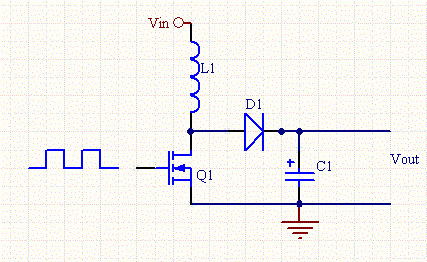
Boost Switching Converter Design Equations
VD represents the voltage drop across the diode, while VTrans indicates the voltage drop across the transistor. The boundary between continuous and discontinuous operation occurs when the output current (io) is zero. A primary consideration in converter design is the...

Full-wave rectifying circuit charging Adjustable
The adjustment potentiometer RP can modify the charging current.
The adjustment potentiometer, designated as RP, serves a critical role in regulating the charging current within an electronic circuit. This component is typically a variable resistor that allows for fine-tuning of the...

By single-phase active power factor correction (APFC) Make up three-phase APF
Tape isolate single-phase power factor correction (PFC) that utilizes DC/DC converters, consisting of two cables. The three-phase PFC is formed by connecting three single-phase PFCs in parallel at the output. This configuration is based on a matrix-type DC/DC converter for...