


High current output switching power supply Schematic Diagram
#switching power supply
#high current
#low voltage
#ST2 diac
#relaxation oscillator
#transistor
#DC power supply
#220V AC input
#timing network
#commutation network
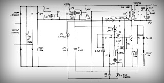
Description: This is a low voltage, high-current output switching DC power supply with an input of 220 volts AC. In this circuit, an ST2 DIAC relaxation oscillator, Q3, C1, and the DIAC initiate conduction of the output switching transistor Q1. The on-time of Q1 is maintained constant by a separate timing and commutation network consisting of Q2, C2, and an SCR. The output voltage is consequently independent of the duty cycle. To compensate for unwanted variations in output voltage due to fluctuations in input voltage or load resistance, an H11C is wired as a linear model unilateral PNP transistor in a stable differential amplifier configuration, which is connected into the galvanically isolated negative feedback loop.
The described circuit operates as a low voltage, high-current output switching DC power supply, designed to convert 220 volts AC input into a regulated DC output. The core of the circuit relies on a DIAC relaxation oscillator, which is crucial for initiating the conduction of the output switching transistor, designated as Q1. The role of Q1 is to control the flow of current to the load, and its on-time is managed by a timing and commutation network that includes Q2, C2, and an SCR. This network ensures that Q1 operates within a specific time frame, which is essential for maintaining consistent performance.
The output voltage remains stable and is largely unaffected by variations in the duty cycle, a significant advantage in applications where load conditions may change frequently. To further enhance the stability of the output voltage, the circuit incorporates an H11C optoisolator configured as a linear model unilateral PNP transistor. This component plays a vital role in the feedback loop, providing galvanic isolation while ensuring that any fluctuations in input voltage or load resistance are compensated for effectively.
The schematic diagram accompanying this description illustrates the arrangement of components and their interconnections, which are critical for the proper functioning of the power supply. The design emphasizes reliability and efficiency, making it suitable for various applications requiring stable high-current DC output.This is low voltage high-current ouput, switching dc power supplly wiht input 220 Volts AC, In this circuit, an St2 diac relaxation oscilator, Q3, C1, and the diac, initiates conduction of the output switching transistor Q1, the on time of which is maintained constant by a separate timing / commutation network consisting of Q2, C2, SUS, an d SCR 1. See schmeatic diagram below : The output voltage, consequently, is independent on the duty cycle. To compensate for unwanted variations of output voltage because of input voltage or load resistance fluctuations, an H11C wired as a liniear - model unilateral pnp transistor in a stable different amplifier configuration is connected into the galvanically isolated negative- feedback loop. You are reading the Circuits of High current output switching power supply And this circuit permalink url it is
The described circuit operates as a low voltage, high-current output switching DC power supply, designed to convert 220 volts AC input into a regulated DC output. The core of the circuit relies on a DIAC relaxation oscillator, which is crucial for initiating the conduction of the output switching transistor, designated as Q1. The role of Q1 is to control the flow of current to the load, and its on-time is managed by a timing and commutation network that includes Q2, C2, and an SCR. This network ensures that Q1 operates within a specific time frame, which is essential for maintaining consistent performance.
The output voltage remains stable and is largely unaffected by variations in the duty cycle, a significant advantage in applications where load conditions may change frequently. To further enhance the stability of the output voltage, the circuit incorporates an H11C optoisolator configured as a linear model unilateral PNP transistor. This component plays a vital role in the feedback loop, providing galvanic isolation while ensuring that any fluctuations in input voltage or load resistance are compensated for effectively.
The schematic diagram accompanying this description illustrates the arrangement of components and their interconnections, which are critical for the proper functioning of the power supply. The design emphasizes reliability and efficiency, making it suitable for various applications requiring stable high-current DC output.This is low voltage high-current ouput, switching dc power supplly wiht input 220 Volts AC, In this circuit, an St2 diac relaxation oscilator, Q3, C1, and the diac, initiates conduction of the output switching transistor Q1, the on time of which is maintained constant by a separate timing / commutation network consisting of Q2, C2, SUS, an d SCR 1. See schmeatic diagram below : The output voltage, consequently, is independent on the duty cycle. To compensate for unwanted variations of output voltage because of input voltage or load resistance fluctuations, an H11C wired as a liniear - model unilateral pnp transistor in a stable different amplifier configuration is connected into the galvanically isolated negative- feedback loop. You are reading the Circuits of High current output switching power supply And this circuit permalink url it is

Full on transistor/fet curve tracer
The project involves adapting a curve tracer schematic, likely based on Metzger's circuit from the early 1970s, to integrate an ADC capture system and output the data to a 320x256 ELD panel. Additionally, a serial output will be included to...

audio tone control 2 transistor circuit
The first BC109C transistor functions as a buffer, delivering a high input impedance of approximately 250k and exhibiting a voltage gain marginally below unity. Given that the Baxendall tone control circuit operates passively, it attenuates all audio frequencies. The audio...

Push-on-push-off electronic switch
Transistors Q1 and Q2 form a flip-flop configuration, while Q3 operates a reed relay. Upon initial power application to the circuit, Q1 and Q3 are in a conducting state, whereas Q2 remains off. A momentary closure of switch S1 triggers...

15 Watt switching power supply
A 15 Watt switching power supply schematic diagram features a pulse transformer T1 constructed on a ferrite core M2500NMS-2 or M2000NM9, with a Sh5h5 size (cross-section of the magnetic coils at the location of 5G—5 mm with a gap in...

Simple Transistor Amplifier Circuit Schematic and Explanation
This circuit does not function as effectively as it could. It was created when the designer had a limited understanding of circuit design. An improved schematic will be developed and posted later, featuring a better design. The schematic indicates "antenna,"...

Simple Two-Transistor Motorcycle Alarm
When one of the switches is closed, the base of Q1 is connected to ground through D1 and R2. This activates Q1, which in turn activates Q2. Q2 connects the positive side of the relay coil to the supply line,...

Transistor Tester
This circuit can measure both small signal hfe and DC current gain hFE of a low to medium power transistor.
The circuit is designed to evaluate the current gain characteristics of low to medium power transistors by measuring both the small...

Transistor Tutorial Power Amplifiers Part 4
An audio power amplifier can enhance weak signals from devices like tuners, CD players, or tape decks to fill a room with sound. This article emphasizes the operating principles and circuitry of low-frequency power amplifiers utilizing bipolar junction transistors (BJTs)....

Parallel DC power supply circuit
A DC power supply with a shunt, rectifier, filter, current limiting, and voltage regulation, providing 10V voltage outputs. The circuit is simple and low cost, designed to meet the requirements of various applications. Additionally, it features a 3V indicator (EL1,...