


70Mhz Rf Power Amplifier Circuit
#RF amplifier
#power amplifier
#SD1143 transistor
#70MHz
#transverter
#high gain
#175MHz device
#14dB gain

Description: The SD1143 transistor offers a gain of approximately 14 dB in this circuit. Its design takes advantage of the fact that a 175-MHz device exhibits significantly higher gain when operated at lower frequencies. The amplifier was initially intended for use with a transverter. The output power ranges from 8 to 10 W for an input of 300 to 500 mW.
The SD1143 transistor is a high-frequency device that excels in low-frequency applications, making it suitable for various amplification tasks. In this circuit configuration, the transistor operates within its optimal gain range, leveraging its characteristics to enhance signal strength effectively. The 14 dB gain indicates that the output signal is 14 times more powerful than the input, which is critical for applications needing robust signal amplification.
The circuit is designed to take a modest input power of 300 to 500 mW and amplify it to a substantial output power of 8 to 10 W. This level of amplification is particularly beneficial in transverter applications, where the signal must be boosted before transmission or further processing. The efficiency of the SD1143 in this role allows for effective communication over extended distances, making it an essential component in RF (radio frequency) systems.
The design considerations for this circuit include the careful selection of passive components, such as resistors and capacitors, to ensure stability and minimize distortion. Proper biasing of the transistor is also crucial to maintain linear operation and prevent thermal runaway. Additionally, attention must be paid to the layout of the circuit to reduce parasitic inductance and capacitance, which can adversely affect performance at higher frequencies.
Thermal management is another important aspect of the circuit design, as the transistor will generate heat during operation. Adequate heat sinking and ventilation must be implemented to ensure reliable operation and longevity of the SD1143 transistor within the circuit. Overall, this amplifier circuit represents a well-engineered solution for achieving significant power amplification in RF applications. The SD1143 transistor provides a gain of about 14 dB in this circuit. It uses the fact that a 175-MHz device has a much higher gain when used at lower frequencies. The amplifier was originally designed to be used with a transverter. The output is 8 to 10 W for a 300- to 500-mW input.
The SD1143 transistor is a high-frequency device that excels in low-frequency applications, making it suitable for various amplification tasks. In this circuit configuration, the transistor operates within its optimal gain range, leveraging its characteristics to enhance signal strength effectively. The 14 dB gain indicates that the output signal is 14 times more powerful than the input, which is critical for applications needing robust signal amplification.
The circuit is designed to take a modest input power of 300 to 500 mW and amplify it to a substantial output power of 8 to 10 W. This level of amplification is particularly beneficial in transverter applications, where the signal must be boosted before transmission or further processing. The efficiency of the SD1143 in this role allows for effective communication over extended distances, making it an essential component in RF (radio frequency) systems.
The design considerations for this circuit include the careful selection of passive components, such as resistors and capacitors, to ensure stability and minimize distortion. Proper biasing of the transistor is also crucial to maintain linear operation and prevent thermal runaway. Additionally, attention must be paid to the layout of the circuit to reduce parasitic inductance and capacitance, which can adversely affect performance at higher frequencies.
Thermal management is another important aspect of the circuit design, as the transistor will generate heat during operation. Adequate heat sinking and ventilation must be implemented to ensure reliable operation and longevity of the SD1143 transistor within the circuit. Overall, this amplifier circuit represents a well-engineered solution for achieving significant power amplification in RF applications. The SD1143 transistor provides a gain of about 14 dB in this circuit. It uses the fact that a 175-MHz device has a much higher gain when used at lower frequencies. The amplifier was originally designed to be used with a transverter. The output is 8 to 10 W for a 300- to 500-mW input.
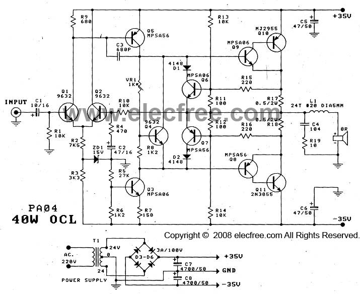
Power Amplifier OCL 40W by 2N3055+MJ2955
The 40W OCL amplifier using the 2N3055 and MJ2955 transistors is simple to construct and cost-effective. It requires a power supply of +35V and -35V with a current rating of 2A. The transistors 2N3055 and MJ2955 must be mounted on...

LM4561 LM4562 consisting of 170W power amplifier circuit
Figure (a) illustrates a 170W output amplifier circuit designed for a 4-ohm load. The LM4651 is a class D amplifier presented in a 28-pin DIP package, with its internal equivalent circuit depicted in Figure (c).
The 170W output amplifier circuit is...

TMB-1 Tri-Mode Buffer Amplifier Box
The TMB-1 is an RF amplifier unit and receiving accessory compatible with low-impedance broadband loops, high-impedance terminated loops (such as Pennant, Flag, or Kaz Delta), and whip (telescoping rod) antennas. This design is optimized for operation within the frequency range...

20w rf fm amplifier circuit
This FM RF amplifier utilizes two transistors from Philips: the BLV 10 and the BLW 87. The two RF transistors are configured in a chic C arrangement, providing an overall gain of 21 dB (100 times) with an efficiency of...

Power amplifier for Loudspeaker 6.5W 8R circuit
The amplifier circuit utilizes negative current feedback, which ensures that the load current is primarily influenced by the input signal rather than the loudspeaker's impedance. The inductor current from the loudspeaker generates a voltage across resistor R7, which is fed...

RF amplifier and filter for 70 MHz
The RF amplifier utilizes noiseless feedback via the drain-gate capacitance, incorporating an inductor in the source lead to achieve the required 90-degree phase shift between the gate voltage and channel current.
The RF amplifier is designed to enhance signal strength while...

Composite CPI amplifier
B is a pure output Class B mode power amplifier. The preamplifier input section of the circuit does not utilize a conventional differential input circuit; instead, it employs a single-ended input. This design features a single-ended output Composite CPI, which...

TV RF Amplifier 5W Circuit With BLW98
The circuit is designed for driving small UHF TV transmitters, providing a gain of 7 dB and capable of amplifying signals within the frequency range of 470-860 MHz. Key components include resistors, capacitors, and transistors.
This circuit serves as a critical...

60 watt 2n3055 power amplifier
This architecture allows for a wide tolerance in component selection, enabling the use of various components that may be readily available. The transistors utilized can be any NPN type power transistor, excluding Darlington configurations. The output power is approximately 60W....