


AM Modulator
#AM modulation
#signal generator
#RF carrier
#audio signal
#LC circuit
#tank circuit
#high frequency
#200kHz
#1kHz
#simulation

Description: This circuit employs two signal generators to simulate an amplitude-modulated RF carrier wave. The output can be utilized to analyze the response of LC and tank circuits. One signal generator represents a high-frequency RF carrier at 200 kHz (VG2), while the other injects a 1 kHz audio signal. The two signals are mixed and amplified by a transistor, resulting in an amplitude-modulated signal appearing at the collector of the BC548 transistor. A capacitor (C2) and resistor (R3) are used to remove the DC component, allowing the RF output to be observed across the load resistor R3. Waveforms are generated using Tina software. To produce an output in Spice Opus, the program must be started, and the new vmod.cir file loaded. The modulated signal can be monitored across R3, which is designated as node 3 relative to ground. After loading the circuit, the "listing" command will display the netlist, while the "run" command simulates the circuit. The "display" command will print a list of all circuit variables, and the command "plot v(3)" will visualize the AM wave between node 3 and ground, specifically across the load resistor R3. To expedite simulation, the RF carrier frequency is limited to 200 kHz, and the output waveform illustrates two complete cycles of the audio wave, corresponding to a duration of 2 ms, given that the modulating frequency is 1 kHz. Additional Spice tutorials will be available on the associated pages.
The circuit is designed to demonstrate amplitude modulation (AM) using two distinct signal generators. The first generator, VG2, produces a high-frequency RF carrier signal at 200 kHz, which serves as the primary signal for modulation. The second generator introduces a low-frequency audio signal at 1 kHz, which modulates the amplitude of the RF carrier.
The mixing of these two signals occurs within the transistor stage, specifically using a BC548 transistor, which is configured to amplify the combined signals. The output at the collector of the transistor is an amplitude-modulated signal, where the amplitude variations correspond to the 1 kHz audio signal, effectively encoding the audio information onto the RF carrier.
To eliminate any DC offset from the output, a coupling capacitor (C2) is employed in conjunction with a resistor (R3). This configuration ensures that only the varying AC component of the modulated signal is present across the load resistor R3, allowing for a clear observation of the AM waveform.
For simulation purposes, the circuit can be analyzed using Tina software, which provides a platform for visualizing the waveforms generated by the circuit. In addition, Spice Opus can be utilized for further simulation and analysis. Upon initiating Spice Opus and loading the vmod.cir file, users can execute commands to display the netlist, simulate the circuit, and visualize the output waveform.
The command sequence facilitates a comprehensive analysis of the circuit's performance, with specific emphasis on the AM wave characteristics observed at node 3. The limitation of the RF carrier frequency to 200 kHz is a strategic choice to simplify the simulation process, while the output waveform is designed to illustrate two complete cycles of the audio modulation, providing a clear representation of the system's functionality.This circuit uses two signal generators to simulate an Amplitude Modulated RF carrier wave. The output can be used to simulate the response of LC and tank circuits. Two signal generators are used in this circuit, one representing a high frequency (200kHz) RF carrier, VG2, the other signal generator is used to inject a 1KHz audio signal. The two si gnals are mixed and amplified by the transistor and an amplitude modulated signal appears at the collector of the BC548. The DC component is removed by C2 and R3 and the RF output now appears across the load resistor R3. Waveforms below are produced using Tina. To produce an output in Spice Opus start the program and load the new vmod. cir The modulated signal appears across R3 which is now node 3 and earth. After loading the circuit the command "listing" will display the netlist. The command "run" will then simulate the circuit, "display" will print a list of all variables in the circuit.
The command plot v(3) will display the AM wave between node 3 and 0 i. e. the load resistor R3. Note to speed up simulation, the RF carrier has been limited to 200KHz only, and the output waveform just shows two complete cycles of the audio wave, i. e. 2ms as the modulating frequency is 1k. There will be some spice tutorials shortly on my pages.
The circuit is designed to demonstrate amplitude modulation (AM) using two distinct signal generators. The first generator, VG2, produces a high-frequency RF carrier signal at 200 kHz, which serves as the primary signal for modulation. The second generator introduces a low-frequency audio signal at 1 kHz, which modulates the amplitude of the RF carrier.
The mixing of these two signals occurs within the transistor stage, specifically using a BC548 transistor, which is configured to amplify the combined signals. The output at the collector of the transistor is an amplitude-modulated signal, where the amplitude variations correspond to the 1 kHz audio signal, effectively encoding the audio information onto the RF carrier.
To eliminate any DC offset from the output, a coupling capacitor (C2) is employed in conjunction with a resistor (R3). This configuration ensures that only the varying AC component of the modulated signal is present across the load resistor R3, allowing for a clear observation of the AM waveform.
For simulation purposes, the circuit can be analyzed using Tina software, which provides a platform for visualizing the waveforms generated by the circuit. In addition, Spice Opus can be utilized for further simulation and analysis. Upon initiating Spice Opus and loading the vmod.cir file, users can execute commands to display the netlist, simulate the circuit, and visualize the output waveform.
The command sequence facilitates a comprehensive analysis of the circuit's performance, with specific emphasis on the AM wave characteristics observed at node 3. The limitation of the RF carrier frequency to 200 kHz is a strategic choice to simplify the simulation process, while the output waveform is designed to illustrate two complete cycles of the audio modulation, providing a clear representation of the system's functionality.This circuit uses two signal generators to simulate an Amplitude Modulated RF carrier wave. The output can be used to simulate the response of LC and tank circuits. Two signal generators are used in this circuit, one representing a high frequency (200kHz) RF carrier, VG2, the other signal generator is used to inject a 1KHz audio signal. The two si gnals are mixed and amplified by the transistor and an amplitude modulated signal appears at the collector of the BC548. The DC component is removed by C2 and R3 and the RF output now appears across the load resistor R3. Waveforms below are produced using Tina. To produce an output in Spice Opus start the program and load the new vmod. cir The modulated signal appears across R3 which is now node 3 and earth. After loading the circuit the command "listing" will display the netlist. The command "run" will then simulate the circuit, "display" will print a list of all variables in the circuit.
The command plot v(3) will display the AM wave between node 3 and 0 i. e. the load resistor R3. Note to speed up simulation, the RF carrier has been limited to 200KHz only, and the output waveform just shows two complete cycles of the audio wave, i. e. 2ms as the modulating frequency is 1k. There will be some spice tutorials shortly on my pages.

Signal Generator 20KHz
This function generator IC is specified to work to 20 MHz. So far, this unit works nicely to 50KHz. Since I seldom need signals higher than that, it has taken up a happy home on my workbench and further development...

7MHz high frequency carrier oscillator
The 2SA130 transistor is used in an oscillator circuit with an oscillation frequency of 7 MHz. The power supply voltage is 6V, and the load is a frequency-selective resonant circuit with a quality factor of 600.
The circuit utilizes the 2SA130...

Test Signal Generator
This signal generator uses a three channel DAC to generate Composite video signal (CVBS) and S video signal (Y/C separated) at the same time, left one channel is not used in NTSC format. It is assigned for one of the...

Audio-frequency generator circuit
An audio frequency signal generator can output audio signals, 465 kHz spectral amplitude signals, and 52.5 Hz to 16 kHz high-frequency amplitude-modulated signals. The high-frequency oscillator's vibration frequency is determined by the components G and L. A variety of musical...

Audio signal control circuit
Audio signal control circuit. It illustrates a typical audio signal control circuit where two audio signals enter the integrated circuit through switching and tone controls (treble and bass), subsequently adjusting the output sent to the audio power amplifier.
The audio signal...

Variety of signal generator circuit
The audio function generator integrated circuit ICL8038 is capable of producing square waves, triangle waves, and sine waves. The electrical resistance and potentiometer RP1 are utilized to determine the 8-pin DC potential Ua, which is typically set to 2Ucr/3. A...
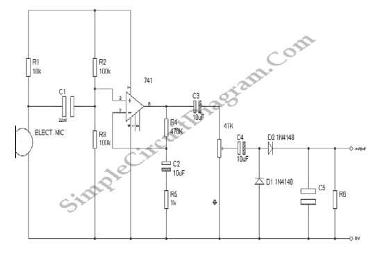
Audio Signal Strength Detector/Converter
Below is the schematic diagram of an audio input module. This module is capable of producing a DC output voltage that is proportional to the amplitude of the input signal.
The audio input module typically consists of several key components that...

450 800Hz signal generator circuit diagram
The 450/800Hz oscillation circuit depicted in the figure utilizes transformer coupling. The frequency conversion is achieved by varying the inductance through a variable filter tap (T1). When the switch control signal (S) is set to position 1, the oscillator circuit...
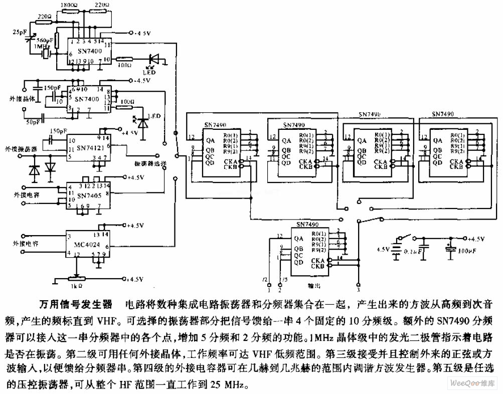
The Multi-purpose signal generator circuit
The multi-purpose signal generator circuit consists of integrated circuit oscillators and frequency dividers. It generates square waves ranging from high frequencies to sub-audio frequencies and also produces a frequency standard in the VHF range. The alternative oscillator section feeds the...