


AM power transmitter
#AM transmitter
#ceramic resonator
#3.587 MHz
#tank circuit
#modulation
#RF output
#transistor
#oscillator
#gang condenser

Description: The circuit for a powerful AM transmitter using ceramic resonator/filter of 3.587 MHz is presented here. Resonators/filters of other frequencies such as 5.5 MHz, 7 MHz and 10.7 MHz may also be used. Use of different frequency filters/resonators will involve corresponding variation in the value of inductor used in the tank circuit of oscillator connected at the collector of transistor T1. The AF input for modulation is inserted in series with emitter of transistor T1 (and resistor R4) using a transistor radio type audio driver transformer as shown in the circuit. Modulated RF output is developed across the tank circuit which can be tuned to resonance frequency of the filter/resonator with the help of gang condenser C7. The next two stages formed using low-noise RF transistors BF495 are, in fact, connected in parallel for amplification of modulated signal coupled from collector of transistor T1 to bases of transistors T2 and T3. The combined output from collectors of T2 and T3 is fed to antenna via 100pF capacitor C4. The circuit can be easily assembled on a general-purpose PCB. The range of the transmitter is expected to be one to two kilometers. The circuit requires regulated 9-volt power supply for its operation. Note: Dotted lined indicates additional connection if a 3-pin filter is used in place.
The described AM transmitter circuit operates primarily at a frequency of 3.587 MHz, utilizing a ceramic resonator or filter. This design allows for flexibility, as resonators or filters of alternative frequencies, such as 5.5 MHz, 7 MHz, and 10.7 MHz, can be integrated. However, it is crucial to adjust the inductor value within the tank circuit of the oscillator, which is connected to the collector of the primary transistor, T1, to accommodate the different frequencies.
The modulation process begins with the audio frequency (AF) input, which is introduced in series with the emitter of transistor T1 and resistor R4. This configuration employs a transistor radio-type audio driver transformer, facilitating effective modulation of the RF signal. The tank circuit, which consists of the inductor and the resonator, is responsible for developing the modulated RF output. The tuning of this output to the resonant frequency is achieved through a gang condenser, denoted as C7 in the schematic.
Subsequent amplification stages utilize low-noise RF transistors, specifically the BF495 model. These transistors, T2 and T3, are configured in parallel to amplify the modulated signal received from the collector of transistor T1. The output from the collectors of T2 and T3 is then routed to the antenna through a coupling capacitor, C4, rated at 100 pF. This design ensures that the amplified signal is effectively transmitted.
The assembly of this circuit is straightforward, as it can be constructed on a general-purpose printed circuit board (PCB), making it accessible for hobbyists and professionals alike. The expected transmission range of this AM transmitter is estimated to be between one to two kilometers, depending on environmental factors and antenna design. A regulated 9-volt power supply is necessary for the operation of the circuit, ensuring stable performance. Additionally, it is noted that a dotted line in the schematic indicates an optional connection for a 3-pin filter, which can be employed in place of the standard configuration.The circuit for a powerful AM transmitter using ceramic resonator/filter of 3.587 MHz is presented here. Resonators/filters of other frequencies such as 5.5 MHz, 7 MHz and 10.7 MHz may also be used. Use of different frequency filters/resonators will involve corresponding variation in the value of inductor used in the tank circuit of oscillator connected at the collector of transistor T1.
The AF input for modulation is inserted in series with emitter of transistor T1 (and resistor R4) using a transistor radio type audio driver transformer as shown in the circuit. Modulated RF output is developed across the tank circuit which can be tuned to resonance frequency of the filter/resonator with the help of gang condenser C7.
The next two stages formed using low-noise RF transistors BF495 are, in fact, connected in parallel for amplification of modulated signal coupled from collector of transistor T1 to bases of transistors T2 and T3. The combined output from collectors of T2 and T3 is fed to antenna via 100pF capacitor C4. The circuit can be easily assembled on a general-purpose PCB. The range of the transmitter is expected to be one to two kilometers. The circuit requires regulated 9-volt power supply for its operation. Note: Dotted lined indicates additional connection if a 3-pin filter is used in place.
The described AM transmitter circuit operates primarily at a frequency of 3.587 MHz, utilizing a ceramic resonator or filter. This design allows for flexibility, as resonators or filters of alternative frequencies, such as 5.5 MHz, 7 MHz, and 10.7 MHz, can be integrated. However, it is crucial to adjust the inductor value within the tank circuit of the oscillator, which is connected to the collector of the primary transistor, T1, to accommodate the different frequencies.
The modulation process begins with the audio frequency (AF) input, which is introduced in series with the emitter of transistor T1 and resistor R4. This configuration employs a transistor radio-type audio driver transformer, facilitating effective modulation of the RF signal. The tank circuit, which consists of the inductor and the resonator, is responsible for developing the modulated RF output. The tuning of this output to the resonant frequency is achieved through a gang condenser, denoted as C7 in the schematic.
Subsequent amplification stages utilize low-noise RF transistors, specifically the BF495 model. These transistors, T2 and T3, are configured in parallel to amplify the modulated signal received from the collector of transistor T1. The output from the collectors of T2 and T3 is then routed to the antenna through a coupling capacitor, C4, rated at 100 pF. This design ensures that the amplified signal is effectively transmitted.
The assembly of this circuit is straightforward, as it can be constructed on a general-purpose printed circuit board (PCB), making it accessible for hobbyists and professionals alike. The expected transmission range of this AM transmitter is estimated to be between one to two kilometers, depending on environmental factors and antenna design. A regulated 9-volt power supply is necessary for the operation of the circuit, ensuring stable performance. Additionally, it is noted that a dotted line in the schematic indicates an optional connection for a 3-pin filter, which can be employed in place of the standard configuration.The circuit for a powerful AM transmitter using ceramic resonator/filter of 3.587 MHz is presented here. Resonators/filters of other frequencies such as 5.5 MHz, 7 MHz and 10.7 MHz may also be used. Use of different frequency filters/resonators will involve corresponding variation in the value of inductor used in the tank circuit of oscillator connected at the collector of transistor T1.
The AF input for modulation is inserted in series with emitter of transistor T1 (and resistor R4) using a transistor radio type audio driver transformer as shown in the circuit. Modulated RF output is developed across the tank circuit which can be tuned to resonance frequency of the filter/resonator with the help of gang condenser C7.
The next two stages formed using low-noise RF transistors BF495 are, in fact, connected in parallel for amplification of modulated signal coupled from collector of transistor T1 to bases of transistors T2 and T3. The combined output from collectors of T2 and T3 is fed to antenna via 100pF capacitor C4. The circuit can be easily assembled on a general-purpose PCB. The range of the transmitter is expected to be one to two kilometers. The circuit requires regulated 9-volt power supply for its operation. Note: Dotted lined indicates additional connection if a 3-pin filter is used in place.

Simple AM Transmitter circuit
This AM transmitter is designed for simplicity, featuring an untapped inductor with a single winding. The inductor can be easily sourced as a standard RF choke, such as the Jaycar Cat LF-1536. To minimize the circuit size, a conventional tuning...
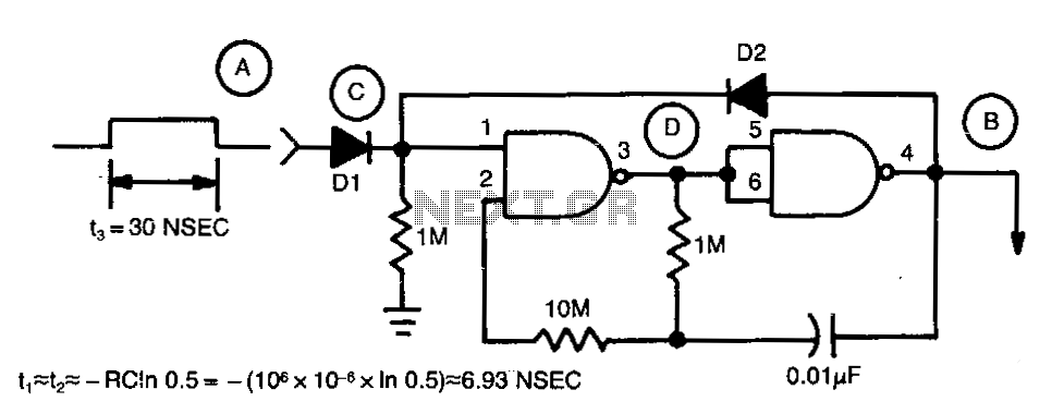
Last-cycle-completing-gated-oscillator
Regenerative feedback at capacitor C allows the oscillator to complete its timing cycle instead of shutting off immediately. The integrated circuit (IC) used was a CD4011AE, although an equivalent IC will also function.
The described circuit utilizes regenerative feedback to enhance...

Camera flash circuit
A simple transistor generator and transformer converts a 1.5V battery voltage to several hundred volts. This high voltage current then passes through a diode, which rectifies the current to DC. This DC current is stored in a relatively large capacitor....

AM Broadcast Transmitter schematic
In this circuit, a 74HC14 hex Schmitt trigger inverter is used as a square wave oscillator to drive a small signal transistor in a class C amplifier configuration. The oscillator frequency can be either fixed by a crystal or made...

Vehicle Detector
A simple single-transistor Colpitts oscillator is depicted in the schematic. When a vehicle passes over the loop, the inductance decreases, resulting in an increase in the oscillator frequency. A microprocessor measures the oscillator frequency and takes appropriate actions based on...

Power Control
The circuit presented utilizes a two-transistor "flasher" to generate triggering pulses, replacing the traditional unijunction transistor design. This configuration allows for a broad range of control with minimal hysteresis and sensitivity to line voltage. Two diodes rectify the line voltage,...

Economical Transistor Radio
The schematic diagram illustrates an audio stage utilizing a common-collector circuit. This configuration does not dampen the tuned circuit; rather, it enhances its response, resulting in improved sensitivity and selectivity. Due to the low supply voltage, the subsequent audio amplifier...

touch switch circuit with 3 transistors
This document describes a series of touch switches that utilize only three transistors. These touch-based transistor switches can activate a load simply by the user touching a metal plate. They are designed to directly switch a relay, enabling operation with...

Single-junction transistor trigger circuit 2
Due to the increased level of the transistor amplifier circuit, the control circuit's performance in Figure 16-6 is more sensitive and can accept input control signals superimposed on others (such as voltage, current, and speed feedback signals) to meet system...