


AVR LED RF Field Strength
#RF field strength
#transmitter tune-up
#RF sniffer
#square law detector
#microcontroller
#LED driver
#A-to-D converter
#two-transistor circuit
#battery voltage stabilization

Description: Useful as a transmitter tune-up meter or an RF sniffer, this is an RF field strength indicator that is loosely based on the Broad Band RF Field Strength Probe, described elsewhere. It detects RF via a square law detector, basically it's a crystal set with gain. The bias circuit for the detector is significantly modified from the probe to reduce the effects of battery voltage droop during use. The circuit contains a small analog section and LED driver, tied together by the microcontroller. A two-transistor circuit provides a stabilized voltage and serves as a detector that serves an A-to-D converter based on the comparator contained in the microcontroller. The voltage from the RF detector is measured once every 160 milliseconds and after removing the zero offset, correcting the polarity (higher field strength results in lower voltage from the detector), overflow detection and formatting to BCD, the microcontroller provides drive signals to the three-digit LED display, which is refreshed once every 16 ms, with a dwell time of about 4 ms per character. This is a little slow for a handheld device as when the meter is moved, a trail of digits is left on the user's retina, so if this bothers you, increase the refresh rate. Q1 is a combination shunt regulator and bias source for Q2. As a shunt regulator, it provides a stabilized voltage for the A-D converter circuit. This shunt regulator has low loop gain, thus the display may jitter because this voltage affects the RF detector's output voltage and power supply fluctuations resulting from driving the LEDs may result in feedback that causes the readings to fluctuate. This could be improved by using a band gap reference ahead of the shunt regulator, but it drives cost and complexity up. I have found the circuit to work erratically when using some batteries - these were some very cheap carbon-zinc and (supposedly) Ni-MH cells that were counterfeits of name brands I bought in S.E. Asia. I suspect these cells have a relatively high impedance, though I did not confirm this experimentally. Name-brand (real ones) alkaline and Ni-Cad batteries don't have these problems. The base voltage on Q1 also serves to establish the bias voltage for Q2's base. Q2 serves as an RF detector. Q1 is biased so that there is about 600 millivolts between its collector and emitter. A small wire antenna forms a capacitive coupling from the input of the circuit to the RF source being observed while the bulk of the circuit, including the battery holder forms a capacitive coupling from the circuit's "ground" to "earth". When the user holds the meter in his or her hand, this ground coupling is enhanced. RF from the small wire antenna is capacitively coupled to Q1's base and this modulates the collector in Q1. Gain of the amplifier is independent of the value of the collector resistor (39K in this case) because that's how transistors work (to use vacuum tube terms, collector signal gain is Gm*Rl, and Gm is nearly proportional to collector current, so doubling the collector load cuts Gm in half). The nonlinearity in the base voltage-to-collector voltage transfer function results in the detection of the RF signal. Collector current is averaged by the low pass filter established by the collector current and the capacitance to ground. The other input to the AT90S2313's on-chip voltage comparator is connected to ramp capacitor C1. The time it takes R1 to charge C1 to equal the voltage from the RF detector (on pin 13 of the AT90S2313) is measured to determine the detector's output. See Atmel's application note, AVR400, for the theory of operation for the A-to-D converter. The power switch is SPDT set up to short the +3V line on the circuit to ground to make sure that the decoupling capacitor was completely discharged so the circuit would reset properly if the power was switched off then back on quickly. This was only done as a precaution and is probably not really necessary. Main features: - Wide bandwidth - Digital display with auto zero - Convenient in that it is self-contained - Very low parts count and low cost - Battery-conserving power management
The RF field strength indicator circuit operates primarily by utilizing a square law detection method, which is effective for measuring radio frequency (RF) signals. The design incorporates a microcontroller, specifically the AT90S2313, which manages the overall operation of the device, including the processing of the RF signal and controlling the display output.
The RF detection process begins with a small wire antenna that captures RF signals from the environment. This antenna couples the RF energy to the base of transistor Q1, which is configured as a shunt regulator and bias source for the second transistor, Q2. Q1's operation is crucial as it stabilizes the voltage supplied to the A-D converter within the microcontroller, ensuring accurate measurements of the incoming RF signal.
The circuit's sensitivity to variations in power supply and component tolerances is addressed by the design of Q1, which maintains a specific bias voltage, approximately 600 millivolts between its collector and emitter. This biasing is essential for the proper functioning of Q2, which acts as the primary RF detector. The gain of the circuit is independent of the collector resistor value, allowing for consistent performance despite variations in component values.
The microcontroller periodically samples the output voltage from the RF detector, applying necessary corrections for zero offset and polarity adjustments. The processed data is then formatted into Binary-Coded Decimal (BCD) for display purposes. The LED display refresh rate is set at 16 ms, which may leave a visual trail when the device is in motion, indicating a potential area for improvement in user experience.
To enhance the performance and reliability of the circuit, especially regarding power supply variations, it is recommended to consider using higher quality batteries with lower internal resistance. This will ensure stable voltage levels and reduce fluctuations that may affect the accuracy of readings.
Overall, the RF field strength indicator is designed to be compact, cost-effective, and efficient, making it a valuable tool for RF enthusiasts and professionals alike. Its low parts count and integrated power management features further contribute to its practicality in various applications, including RF tuning and signal detection.Useful as a transmitter tune-up meter or an RF sniffer, this is an RF field strength indicator that is loosely based on the Broad Band RF Field Strength Probe, described elsewhere. It detects RF via a square law detector, basically its a crystal set with gain. The bias circuit for the detector is significantly modified from the probe to reduce the effects of battery voltage droop during use.
The circuit contains a small analog section and LED driver, tied together by the micro controller. A two-transistor circuit provides a stabilized voltage and serves as a detector that serves an A-to-D converter based on the comparator contained in the micro controller. The voltage from the RF detector is measured once every 160 milliseconds and after removing the zero offset, correcting the polarity (higher field strength results in lower voltage from the detector), overflow detection and formatting to BCD, the micro controller provides drive signals to the three digit LED display, which is refreshed once every 16 ms, with a dwell time of about 4 ms per character.This is a little slow for a handheld device as when the meter is moved, a trail of digits is left on the user's retina, so if this bothers you, increase the refresh rate. Q1 is a combination shunt regulator and bias source for Q2. As a shunt regulator, it provides a stabilized voltage for the A-D converter circuit. This shunt regulator has low loop gain, thus the display may jitter because this voltage affects the RF detector's output voltage and power supply fluctuations resulting from driving the LEDs may result in feedback that causes the readings to fluctuate.
This could be improved by using a band gap reference ahead of the shunt regulator, but it drives cost and complexity up. I have found the circuit to work erratically when using some batteries -these were some very cheap carbon-zinc and (supposedly) Ni-MH cells that were counterfeits of name brands I bought in S.E.
Asia. I suspect these cells have a relatively high impedance, thought I did not confirm this experimentally. Name-brand (real ones) alkaline and Ni-Cad batteries don't have these problems. The base voltage on Q1 also serves to establish the bias voltage for Q2's base. Q2 serves a an RF detector. Q1 is biased so that there is about 600 millivolts between its collector and emitter. A small wire antenna forms a capacitive coupling from the input of the circuit to the RF source being observed while the bulk of the circuit, including the battery holder forms a capacitive coupling from the circuits' "ground" to "earth".
When the user holds the meter in his or her hand, this ground coupling is enhanced. RF from the small wire antenna is capacitively coupled to Q1's base and this modulates the collector in Q1. Gain of the amplifier is independent of the value of the collector resistor (39K in this case) because that's how transistors work (to use vacuum tube terms, collector signal gain is Gm*Rl, and Gm is nearly proportional to collector current, so doubling the collector load cuts Gm in half) .The nonlinearity in the base voltage-to-collector voltage transfer funcion results in detection of the RF signal.
Collector current is averaged by the low pass filter established by the collector current and the capacitance to ground. The other input to the AT90S2313s on-chip voltage comparator is connected to ramp capacitor C1. The time it takes R1 to charge C1 to equal the voltage from the RF detector (on pin 13 of the AT90S2313) is measured to determine the detector's output.
See Atmels' application note, AVR400, for the theory of operation for the A-to-D converter. The power switch is SPDT set up to short the +3V line on the circuit to ground to make sure that the decoupling capacitor was completely discharged so the circuit would reset properly if the power was switched off then back on quickly. This was only done as a precaution and is probably not really necessary. Main features: - Wide bandwidth - Digital display with auto zero - Convenient in that it is self contained - Very low parts count and low cost - Battery-conserving power management Follow the links for information on
The RF field strength indicator circuit operates primarily by utilizing a square law detection method, which is effective for measuring radio frequency (RF) signals. The design incorporates a microcontroller, specifically the AT90S2313, which manages the overall operation of the device, including the processing of the RF signal and controlling the display output.
The RF detection process begins with a small wire antenna that captures RF signals from the environment. This antenna couples the RF energy to the base of transistor Q1, which is configured as a shunt regulator and bias source for the second transistor, Q2. Q1's operation is crucial as it stabilizes the voltage supplied to the A-D converter within the microcontroller, ensuring accurate measurements of the incoming RF signal.
The circuit's sensitivity to variations in power supply and component tolerances is addressed by the design of Q1, which maintains a specific bias voltage, approximately 600 millivolts between its collector and emitter. This biasing is essential for the proper functioning of Q2, which acts as the primary RF detector. The gain of the circuit is independent of the collector resistor value, allowing for consistent performance despite variations in component values.
The microcontroller periodically samples the output voltage from the RF detector, applying necessary corrections for zero offset and polarity adjustments. The processed data is then formatted into Binary-Coded Decimal (BCD) for display purposes. The LED display refresh rate is set at 16 ms, which may leave a visual trail when the device is in motion, indicating a potential area for improvement in user experience.
To enhance the performance and reliability of the circuit, especially regarding power supply variations, it is recommended to consider using higher quality batteries with lower internal resistance. This will ensure stable voltage levels and reduce fluctuations that may affect the accuracy of readings.
Overall, the RF field strength indicator is designed to be compact, cost-effective, and efficient, making it a valuable tool for RF enthusiasts and professionals alike. Its low parts count and integrated power management features further contribute to its practicality in various applications, including RF tuning and signal detection.Useful as a transmitter tune-up meter or an RF sniffer, this is an RF field strength indicator that is loosely based on the Broad Band RF Field Strength Probe, described elsewhere. It detects RF via a square law detector, basically its a crystal set with gain. The bias circuit for the detector is significantly modified from the probe to reduce the effects of battery voltage droop during use.
The circuit contains a small analog section and LED driver, tied together by the micro controller. A two-transistor circuit provides a stabilized voltage and serves as a detector that serves an A-to-D converter based on the comparator contained in the micro controller. The voltage from the RF detector is measured once every 160 milliseconds and after removing the zero offset, correcting the polarity (higher field strength results in lower voltage from the detector), overflow detection and formatting to BCD, the micro controller provides drive signals to the three digit LED display, which is refreshed once every 16 ms, with a dwell time of about 4 ms per character.This is a little slow for a handheld device as when the meter is moved, a trail of digits is left on the user's retina, so if this bothers you, increase the refresh rate. Q1 is a combination shunt regulator and bias source for Q2. As a shunt regulator, it provides a stabilized voltage for the A-D converter circuit. This shunt regulator has low loop gain, thus the display may jitter because this voltage affects the RF detector's output voltage and power supply fluctuations resulting from driving the LEDs may result in feedback that causes the readings to fluctuate.
This could be improved by using a band gap reference ahead of the shunt regulator, but it drives cost and complexity up. I have found the circuit to work erratically when using some batteries -these were some very cheap carbon-zinc and (supposedly) Ni-MH cells that were counterfeits of name brands I bought in S.E.
Asia. I suspect these cells have a relatively high impedance, thought I did not confirm this experimentally. Name-brand (real ones) alkaline and Ni-Cad batteries don't have these problems. The base voltage on Q1 also serves to establish the bias voltage for Q2's base. Q2 serves a an RF detector. Q1 is biased so that there is about 600 millivolts between its collector and emitter. A small wire antenna forms a capacitive coupling from the input of the circuit to the RF source being observed while the bulk of the circuit, including the battery holder forms a capacitive coupling from the circuits' "ground" to "earth".
When the user holds the meter in his or her hand, this ground coupling is enhanced. RF from the small wire antenna is capacitively coupled to Q1's base and this modulates the collector in Q1. Gain of the amplifier is independent of the value of the collector resistor (39K in this case) because that's how transistors work (to use vacuum tube terms, collector signal gain is Gm*Rl, and Gm is nearly proportional to collector current, so doubling the collector load cuts Gm in half) .The nonlinearity in the base voltage-to-collector voltage transfer funcion results in detection of the RF signal.
Collector current is averaged by the low pass filter established by the collector current and the capacitance to ground. The other input to the AT90S2313s on-chip voltage comparator is connected to ramp capacitor C1. The time it takes R1 to charge C1 to equal the voltage from the RF detector (on pin 13 of the AT90S2313) is measured to determine the detector's output.
See Atmels' application note, AVR400, for the theory of operation for the A-to-D converter. The power switch is SPDT set up to short the +3V line on the circuit to ground to make sure that the decoupling capacitor was completely discharged so the circuit would reset properly if the power was switched off then back on quickly. This was only done as a precaution and is probably not really necessary. Main features: - Wide bandwidth - Digital display with auto zero - Convenient in that it is self contained - Very low parts count and low cost - Battery-conserving power management Follow the links for information on

ADP1649 1A LED Flash Driver | ADP1649 Datasheet
The ADP1649 is a compact and highly efficient single white LED flash driver designed for high-resolution camera phones, enhancing the quality of pictures and videos.
The ADP1649 integrates advanced features that optimize the performance of single white LED flash applications. It...

10A High power led driver circuit design using LM3434
The LM3434 adaptive constant on-time DC/DC buck (step-down) constant current controller can be used to design a simple high-power LED driver application. The LM3434 provides a constant current for illuminating high-power LEDs. The output configuration allows the anodes of multiple...

How to Design Battery Charger Applications that Require External Microcontrollers and Related System-Level Issues
Application note on designing linear and switch-mode (switching DC-DC converter current source) battery charger applications that require external microcontrollers and related system-level issues for notebook computers.
The application note provides guidance on the design of both linear and switching DC-DC converter...

LED driver based on MP3302 LED driver IC. Working circuit diagram.Operates from a single Lithium ion battery
The MP3302 is a boost converter integrated circuit (IC) specifically designed for LED drive applications. It is capable of driving 27 LEDs, arranged as 9 strings of 3 white LEDs in series, powered by a lithium-ion battery. The IC features...

Random oscillator circuit for high power LEDs
A circuit is needed to drive three or more LEDs at a current of 200-350mA each, with the capability to randomly flash or strobe them at a frequency of 5-20Hz. The input power should be low-voltage DC, with a preference...
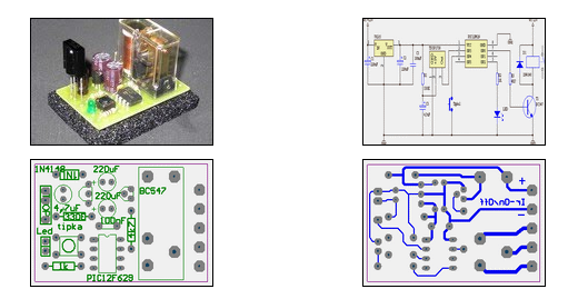
IR On/Off Switch Using Microcontroller
The ability to turn electrical devices ON or OFF using a remote control is a well-established concept, with numerous devices effectively performing this function.
To implement a remote control system for switching electrical devices, a typical schematic would include several key...

Robo Atmega328p project
This project was designed to introduce a friend to microcontrollers and circuits using various functionalities and spare parts. A PS2 numpad was utilized as the key entry mechanism, which was found at a thrift store and included the necessary connector....

Wide Input-Voltage Range High-Power LED Driver
This is a high-power LED driver circuit designed to accommodate a wide input-voltage range. The circuit utilizes a buck/boost converter controller to regulate the current supplied to a white LED.
The high-power LED driver circuit is engineered to effectively manage varying...

GSM Remote Control 2 IN and 2 OUT Part 2 Schematic
The control of the system is managed by a Microchip PIC18F46K20-I/PT microcontroller, which is programmed with firmware to oversee the activity of the GSM/GPRS module, monitor the logic conditions of two opto-isolated inputs, and send commands to two relays within...